1 / 19

E N D
Course: Quantum Electronics Arpan Deyasi Quantum Topic: Quantum Well – mathematical calculation for real structure Electronics Arpan Deyasi Arpan Deyasi, RCCIIT, India 5/9/2020 1
Recapitulation: ‘Particle in a Box’ problem Arpan Deyasi 2 2 d Quantum − + ( ) ( ) V z = ( ) ( ) E z z z * 2 2 m dz for 0<z<L, V(z) = 0 Electronics for z≤0 & z≥L, V(z) = ∞ 2 2 2 n = E n * 2 2 m L L 5/9/2020 Arpan Deyasi, RCCIIT, India 2
Queries Q1: What is the material outside of the well? Arpan Deyasi Q2: How can the potential barrier be infinite? Is it practically realizable? Quantum Q3: How the electron effective mass inside and outside the material be same? Electronics Q4: How step potential configuration be physically realizable? 5/9/2020 Arpan Deyasi, RCCIIT, India 3
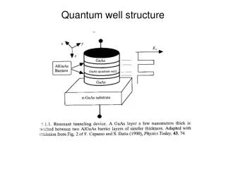
how a quantum well is really formed Arpan Deyasi Quantum Electronics 5/9/2020 Arpan Deyasi, RCCIIT, India 4
how a quantum well is really formed Arpan Deyasi Quantum Electronics 5/9/2020 Arpan Deyasi, RCCIIT, India 5
how carriers are trapped Arpan Deyasi Quantum Electronics Exciton 5/9/2020 Arpan Deyasi, RCCIIT, India 6
Electron motion in a Quantum well Arpan Deyasi ✓Two dimensions are unrestricted Quantum ✓Only one dimension is restricted Electronics 5/9/2020 Arpan Deyasi, RCCIIT, India 7
Electron motion in a Quantum wire Arpan Deyasi ✓Only one dimension are unrestricted Quantum ✓Two dimensions are restricted Electronics 5/9/2020 Arpan Deyasi, RCCIIT, India 8
Electron motion in a Quantum dot Arpan Deyasi ✓All the three dimensions are restricted Quantum Electronics 5/9/2020 Arpan Deyasi, RCCIIT, India 9
Introducing Schrödinger Equation Arpan Deyasi 2 2 ( ) z d + ( ) ( ) V z = ( ) ( ) E z 2m ( ) Quantum - z z * 2 z dz Electronics + 2 1 *( ) ( ) z dz d dz m d ( ) ( ) V z = ( ) ( ) E z - z z 2 z 5/9/2020 Arpan Deyasi, RCCIIT, India 10
Introducing Schrödinger Equation Arpan Deyasi for V=0 Quantum 2 1 *( ) ( ) z dz d dz m Electronics d = ( ) ( ) E z - z 2 z w for V=V0 2 1 *( ) ( ) z dz d dz m d + 0 = ( ) ( ) E z - ( ) z V z 2 z b 5/9/2020 Arpan Deyasi, RCCIIT, India 11
Introducing Schrödinger Equation Arpan Deyasi for V=0 Quantum material parameter * 2 2 ( ) z ( ) z m d + ( ) ( ) E z = 0 z w 2 2 dz Electronics * 2 ( ) z E m = w 1 2 2 ( ) z d 2 + ( ) ( ) z = 0 z 1 2 dz 5/9/2020 Arpan Deyasi, RCCIIT, India 12
Introducing Schrödinger Equation Arpan Deyasi for V=V0 Quantum material parameter * 2 2 ( ) z ( ) z m d ( ) + Electronics − = ( ) ( ) z 0 E z V b 0 2 2 dz 2 * − 2 ( ) z E V m = 0 b 2 2 ( ) z d 2 + ( ) ( ) z = 0 z 2 2 dz 5/9/2020 Arpan Deyasi, RCCIIT, India 13
Introducing Schrödinger Equation Arpan Deyasi κ1: wave-vector of quantum well, i.e., for lower bandgap material Quantum κ2: wave-vector of quantum barrier, i.e., for higher bandgap material Electronics κ1 = f(mw*) ------ material parameter dependence κ2 = f(mb*) ------ material parameter dependence 5/9/2020 Arpan Deyasi, RCCIIT, India 14
Where is the physics of semiconductor device? Arpan Deyasi 2 2 ( ) Quantum + + + = 2 1 ....... E E E * 2 m Electronics band non-parabolicity of first order band non-parabolicity of second order 5/9/2020 Arpan Deyasi, RCCIIT, India 15
Two-Dimensional Electron Gas (2DEG) Arpan Deyasi Quantum Wave nature Electronics Electrons in CB are considered Electrons confined in conduction band of quantum well Quantum well 5/9/2020 Arpan Deyasi, RCCIIT, India 16
Multiple Quantum Well/Superlattice Arpan Deyasi Quantum Electronics 5/9/2020 Arpan Deyasi, RCCIIT, India 17
Q. What is the difference between MQW & Superlattice? Arpan Deyasi Superlattice is a type of Multiple Quantum Well structure where Quantum wavefunctions between adjacent quantum wells Electronics can help carrier transfer through quantum-mechanical tunneling process 5/9/2020 Arpan Deyasi, RCCIIT, India 18
Thickness of the sandwich barrier is critical for tunneling process Arpan Deyasi Quantum Superlattice Electronics MQW but not superlattice 5/9/2020 Arpan Deyasi, RCCIIT, India 19


![[Nonuniform primary photocurrent spreading in quantum well infrared photoconductors]](https://cdn2.slideserve.com/5143935/nonuniform-primary-photocurrent-spreading-in-quantum-well-infrared-photoconductors-dt.jpg)