1 / 30
300 likes | 336 Vues
Brief description of Coulomb blockade and single-electron transistor

E N D
Course: Nanoelectronic Device Arpan Deyasi Nanoelectronic Coulomb Blockade and Single Electron Transistor Device Arpan Deyasi RCCIIT, India 29-05-2021 Arpan Deyasi, RCCIIT, Kolkata 1
Arpan Deyasi Nanoelectronic Coulomb Blockade Device 29-05-2021 Arpan Deyasi, RCCIIT, Kolkata 2
Effect of single electron transfer Arpan Deyasi Nanoelectronic Device Quantum system lead 29-05-2021 Arpan Deyasi, RCCIIT, Kolkata 3
Effect of Single charge transfer A single electron transferred from lead to quantum system Arpan Deyasi Nanoelectronic Redistribution of charge in the lead Device Change in electrostatic potential energy 29-05-2021 Arpan Deyasi, RCCIIT, Kolkata 4
Effect of Single charge transfer For macroscopic system, change of electrostatic energy is negligible (U ≃ ≃ kBT) Arpan Deyasi Nanoelectronic For microscopic system, change of electrostatic energy is significant (U > kBT) Device For microscopic system at low temperature, change of electrostatic energy is very significant (U >> kBT) 29-05-2021 Arpan Deyasi, RCCIIT, Kolkata 5
Coulomb Blockade Arpan Deyasi Large change in electrostatic energy of a system due to transfer of a single carrier results an energy gap in the system, defined as Coulomb blockade Nanoelectronic Blocking of electron tunneling through a junction due to repulsion of electrons by Coulomb field Device Applied bias Energy gap Coulomb island Material and geometry of the quantum structure controls coulomb blockade 29-05-2021 Arpan Deyasi, RCCIIT, Kolkata 6
Criteria of Single charge transfer Arpan Deyasi consider a single tunnel under application of external bias ‘V’ Nanoelectronic 2 q = U energy stored in the tunnel junction Device 2 C Under application of bias V, an electron at source electrode with K.E. ES(κ) will tunnel into the drain electrode with K.E. ED(κ’) 29-05-2021 Arpan Deyasi, RCCIIT, Kolkata 7
Criteria of Single charge transfer Arpan Deyasi energy conservation gives Nanoelectronic − 2 1 2 ( ) CV q ( ) + = ( ') + 2 E CV E S D 2 C satisfying Pauli’s exclusion principle Device ( ') − ( ) ( ) − E E k T ( ) E E k T D F B S F B 29-05-2021 Arpan Deyasi, RCCIIT, Kolkata 8
Criteria of Single charge transfer Arpan Deyasi Inequality conditions together gives Nanoelectronic ( ') − ( )) ( 2 E E k T D S B tunneling condition is given by Device 2 q − 2 qV k T B 2 C 29-05-2021 Arpan Deyasi, RCCIIT, Kolkata 9
Criteria of Single charge transfer Arpan Deyasi Inference: [i] no current can flow at a bias below a threshold voltage which depends on the temperature Nanoelectronic Inference: [ii] At T = 0, no current below Device q C V can flow f This region is called the Coulomb region 29-05-2021 Arpan Deyasi, RCCIIT, Kolkata 10
Criteria of Single charge transfer Arpan Deyasi Inference: [iii] The prohibition of tunneling is called Coulomb blockade Nanoelectronic Inference: [iv] The energy Device 2 q = = qV E is called the Coulomb gap energy C 2 C 29-05-2021 Arpan Deyasi, RCCIIT, Kolkata 11
I-V characteristics indicating Coulomb gap I Arpan Deyasi Nanoelectronic Device -(q/2C) V (q/2C) 29-05-2021 Arpan Deyasi, RCCIIT, Kolkata 12
Criteria for Coulomb Blockade Applied bias should be less than q/C Arpan Deyasi q C V f Nanoelectronic 2 System thermal energy should be less than q2/C Device q C k T B h q R Tunneling resistance should be greater than h/q2 T 2 29-05-2021 Arpan Deyasi, RCCIIT, Kolkata 13
Arpan Deyasi Nanoelectronic Single Electron Transistor Device 29-05-2021 Arpan Deyasi, RCCIIT, Kolkata 14
Criteria for Single Electron Tunneling Arpan Deyasi q C V Applied bias should be greater than q/C Nanoelectronic f 2 System thermal energy should be greater than q2/C Device q C k T B h q R Tunneling resistance should be less than h/q2 T 2 29-05-2021 Arpan Deyasi, RCCIIT, Kolkata 15
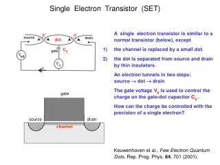
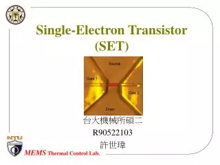
Schematic Structure Arpan Deyasi Gate Nanoelectronic CG Device CD CS Quantum Dot Drain Source RS RD 29-05-2021 Arpan Deyasi, RCCIIT, Kolkata 16
Definition Arpan Deyasi SET is switchingtype of transistor where Nanoelectronic source and drain are quantum-mechanically connected Device throughquantum confined structure (Q. Wire or Q. Dot) that works as channel; and uses controlled electron tunneling for amplificationof current 29-05-2021 Arpan Deyasi, RCCIIT, Kolkata 17
Operating Principle Operation is based on quantum tunneling phenomena Arpan Deyasi By application of bias, electron transfers between source and drain via tunneling mechanism Nanoelectronic Gate potential effectively helps to raise eigenstates of the quantum wire/dot Device 29-05-2021 Arpan Deyasi, RCCIIT, Kolkata 18
Operating Principle Arpan Deyasi In blocking state, no accessible energy levels are within the tunneling range of electron on source contact Nanoelectronic All energy levels of the quantum device with lower energies are occupied Device 29-05-2021 Arpan Deyasi, RCCIIT, Kolkata 19
Operating Principle After application of positive bias, energy levels of the dot are lower. Arpan Deyasi Then one electron can tunnel to the dot, occupying a previously vacant energy levels. Nanoelectronic From there it tunnels to drain. Device 29-05-2021 Arpan Deyasi, RCCIIT, Kolkata 20
MATHEMATICAL MODELING total capacitance of the device is given by Arpan Deyasi = + + C C C C change of free energies at drain and source ends due to nSand nDnumber of electrons flow Nanoelectronic S D G n n Device q q = − + ( , ) { ( ) ( ) } F N Q C C V C V 0 S S D e G D G G 2 C q q = − ( , ) { ( ) } F n n N Q C V C V 0 D S D e S G G 2 C N is the number of electrons in the single dot, and Q0is the background charge 29-05-2021 Arpan Deyasi, RCCIIT, Kolkata 21
MATHEMATICAL MODELING electron tunneling rates Arpan Deyasi Nanoelectronic − 1 F F = ( ) N Device S S 1 exp( − 2 / ) R q k T S S B − 1 F F = ( ) N D D 1 exp( − 2 / ) R q k T D D B 29-05-2021 Arpan Deyasi, RCCIIT, Kolkata 22
MATHEMATICAL MODELING Arpan Deyasi time rate of probability density Nanoelectronic ( , ) N t t + − − + = + + + + − ( )[ N + ( 1)[ ( 1) ( 1)] ( ) N ( )] N N N N D S D S Device Under steady state condition − + + − ( )[ N + = + 1) [ + + + ( ) N ( )] N ( ( 1) ( 1)] N N N D S D S 29-05-2021 Arpan Deyasi, RCCIIT, Kolkata 23
MATHEMATICAL MODELING Arpan Deyasi Boundary condition N → Nanoelectronic Device ( ) N → 0 For normalization ( ) 1 N = =− N 29-05-2021 Arpan Deyasi, RCCIIT, Kolkata 24
MATHEMATICAL MODELING Arpan Deyasi drain current is given by Nanoelectronic ( ) N + − = − ( ) I V [ ( ) N ( )] N q S S =− N Device ( ) N + − = − ( ) I V [ ( ) N ( )] N q D D =− N 29-05-2021 Arpan Deyasi, RCCIIT, Kolkata 25
Arpan Deyasi Nanoelectronic Device 29-05-2021 Arpan Deyasi, RCCIIT, Kolkata 26
Why SET is advantageous? Arpan Deyasi Consumes less power for operation --- reduces circuit power dissipation Nanoelectronic Drawbacks ▪ Operation at Room Temp Device ▪ Fabrication ▪ Charge Offset 29-05-2021 Arpan Deyasi, RCCIIT, Kolkata 27
Application 1. Detection of Infrared Radiation Arpan Deyasi Nanoelectronic Calculation of photo-response of single electron system subject to electromagnetic radiation can be easily determined since tunneling events are uncorrelated Device 29-05-2021 Arpan Deyasi, RCCIIT, Kolkata 28
Application Arpan Deyasi 2. Spectroscopic application If one electron in an otherwise single electron system is added; then the additional energy can easily be distinguished. Nanoelectronic This property is utilized to design ultra-sensitive photodetector. Device 29-05-2021 Arpan Deyasi, RCCIIT, Kolkata 29
Application Arpan Deyasi 3. Programmable Logic Nanoelectronic SET has nonvolatile memory function. Its phase shift can be considered NMOS device for anticlock direction & PMOS device for clockwise direction. Device This helps to form CMOS switch which is the backbone of quantum- mechanical VLSI circuits. 29-05-2021 Arpan Deyasi, RCCIIT, Kolkata 30