Download
1 / 13
130 likes | 229 Vues
Get more information from here -http://www.hitechcircuits.com/pcb-products/heavy-copper-pcb/<br>

E N D
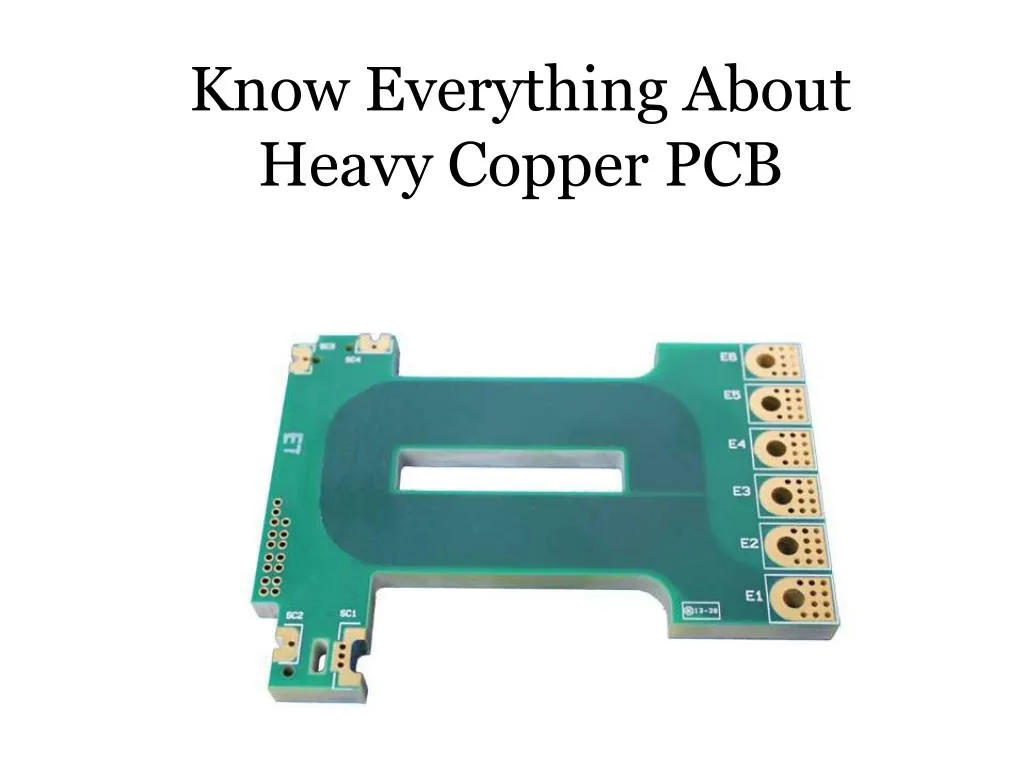
AboutHeavy Copper PCB In these heavy cooper PCBs are very demandable in market. Heavy Copper Printed Circuit Board (PCB) is 3 or more ounces of finished copper in the inner and/or outer layers. It is made using the process of Laminated Deposition.
What Are The Benefits Of Using Heavy Copper In PCB? The capability of heavy copper to survive frequent exposure if there is excessive current, elevated temperatures and recurring thermal cycling that can destroy a regular circuit board in seconds.
The high tolerance capacity of heavy copper makes it compatible with applications in rough situations such as, defense and aerospace industry products.
Compact in product size as the several copper weights are used in the same layer of circuitry.
Interesting Facts About Heavy Copper PCB It is accepted if it the copper is 3 ounces ft2 to 10 oz per ft2 in the outer and inner layers.
It is used on the internal and external layers of a printed circuit board.
Improved copper balances substrate into the holes by changing a weak board into the long-lasting and dependable wiring platform.
You should always check the copper’s thickness during the circuit design stage.
The current-carrying capacity is determined from the width and thickness of heavy copper.
The heavy copper conductor increases the entire PCB thickness.
If you need more information related to Heavy copper PCB then please visit on below website. http://www.hitechcircuits.com/pcb-products/heavy-copper-pcb/