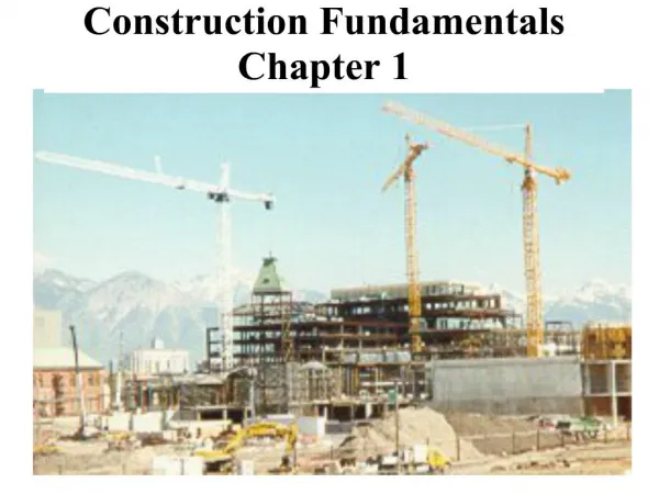
Download
1 / 13
140 likes | 570 Vues
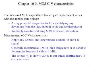
2. MOSFET. P-Si. electrons. . N-channelMOSFET(NMOS)uses p-type substrate. 3. MOSFET operation. VG1. VG2. VG3. VG3 > VG2 > VG1. When a positive voltage VG is applied to the gate relative to the substrate, mobile negative charges (electrons) gets attracted to Si-oxide interface. These induced electrons form the channel.For a given value of VG, the current ID increases with VD, and finally saturates..

E N D
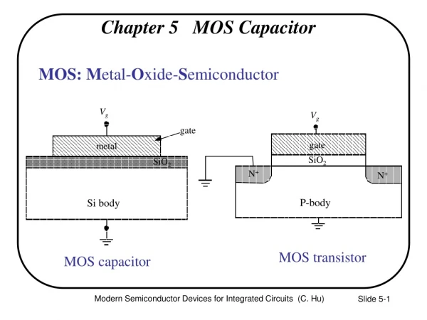
1. 1 Chapter 16-1. MOS fundamentals Metal-oxide-semiconductor FET is the most important device in modern microelectronics.
In this chapter, we will study:
Ideal MOS structure electrostatics
MOS band diagram under applied bias
Gate voltage relationship
capacitance-voltage relationship under low frequency and under high frequency.
2. 2 MOSFET
3. 3 MOSFET operation
4. 4 Ideal MOS capacitor Oxide has zero charge, and no current can pass through it.
No charge centers are present in the oxide or at the oxide-semiconductor interface.
Semiconductor is uniformly doped
?M = ?S
= ? + (EC � EF)FB
5. 5 Equilibrium energy band diagram for an ideal MOS structure
6. 6 Effect of an applied bias Let us ground the semiconductor and start applying different voltages, VG, to the gate
VG can be positive, negative or zero with respect to the semiconductor
EF, metal � EF, semiconductor = � q VG
(Since electron energy = ? q V, when V < 0, electron energy increases)
Since oxide has no charge, d Eoxide / dx = ?/? = 0; i.e. the E-field inside the oxide is constant.
7. 7 Consider p-type Si, apply VG < 0
8. 8 Accumulation condition, VG < 0, p-type Si
9. 9 Consider p-type Si, apply VG > 0 (Depletion condition)
10. 10 Consider p-Si, apply VG >> 0 (Inversion condition)
11. 11 Inversion condition
12. 12 Energy band diagrams and charge density diagrams describing MOS capacitor in n-type Si
13. 13 Energy band diagrams and charge density diagrams describing MOS capacitor in p-type Si
14. 14 Example 1