Download
1 / 13
190 likes | 686 Vues
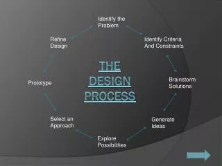
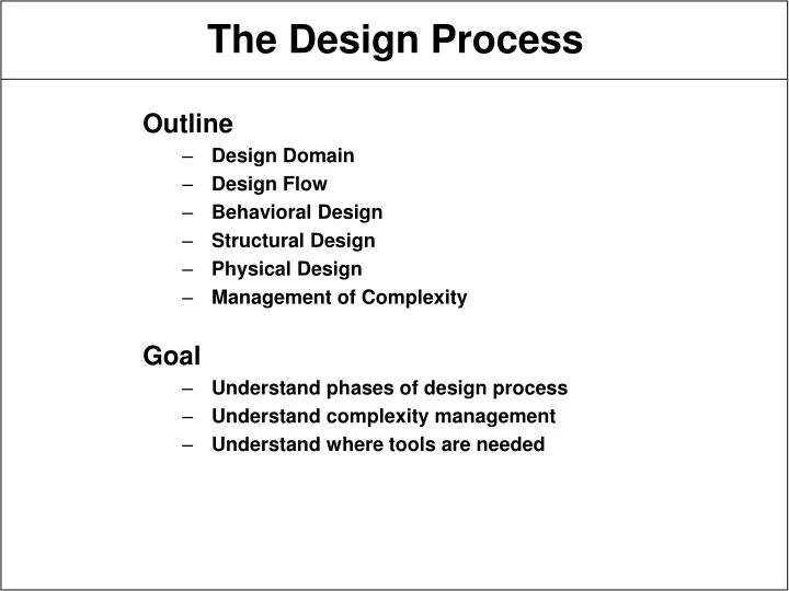
Outline Design Domain Design Flow Behavioral Design Structural Design Physical Design Management of Complexity Goal Understand phases of design process Understand complexity management Understand where tools are needed. The Design Process. Design Domain. Behavioral Domain.

E N D
Outline Design Domain Design Flow Behavioral Design Structural Design Physical Design Management of Complexity Goal Understand phases of design process Understand complexity management Understand where tools are needed The Design Process
Design Domain Behavioral Domain Structural Domain App PMS OS CPU Prog Proc RTL Inst Gate Xistor Process Field Circuit Xistor Logic Cell Architecture Module Board Box Physical Domain
Design Flow Design Specification Verify Function Behavioral Design Sim., DRC Verify Function Mapping Feedback Structural Design Sim., DRC Verification Function Speed, Power Mapping Physical Design Simulation Design Rule Checking Manuf. Data Manufacturing Specification
Design Phase Upper Design Level Map to more detailed design representation. Synthesis Usually just rework design Determine if design meets performance objectives, obeys manufacturing rules. Often contained as part of synthesis tool inner loop. Analysis Reject Might require starting over Determine if equivalent to more abstract design. Human error or tool bug if not. Verification Validation Reject Lower Design Level
Map design spec to formal behavioral description design spec == user desires “a cheap 100MHz Pentium chip” often not formally described design and behavioral spec often developed together Approach use behavioral hardware description language (HDL) Verilog VHDL HDL is programming language superset support for timing, modules verify HDL implements design spec usually through simulation check that HDL is self-consistent “compile” and simulate Behavioral Design
Map behavioral spec to structural spec partition into functional blocks - the netlist targets for eventual physical design Approach use behavioral modules as starting point decompose each block to finer detail function to gates to transistors, etc. stop at manufacturing interface logic design - boolean equations => gates simulation to verify structure has correct behavior interconnect verification design rule checking feedback from physical design - back annotation for performance verification No! Structural Design c = a + b RegA RegB + RegC
Map from structure to physical implementation target technology technology mapping netlist to 2-D layout Approach partition into boards, modules, chips, cells, layout place and route fix cell locations route wiring cell layout design rule checking circuit extraction interconnect verification back annotation Physical Design
Bigger, faster designs have more coupling in design flow more feedback => more design iterations => higher cost simultaneous design => complex tools cannot do “technology independent” design Typical big design 10M transistors 300 MHz clock rate beyond brute force approaches Solutions hierarchy regularity abstraction simplification Management of Complexity
Structure design as you would a program “procedure calls” stop at manufacturing interface - “atoms” of IC universe Hierarchy ALU Shift Reg Mult µP Datapath Cache 1-Bit ALU I/O SRAM Use ALU cell from library • Design SRAM cell by hand •
Use replication behavioral - call same procedure many times structural - instantiate same cell many times physical - instantiate same cell many times Examples bit in SRAM array bit slice in datapath Enhancement module generators procedure call for structural and physical design pitch matching array logic PLA, ROM Regularity
Use most abstract representation possible hide information => less memory simpler representation => less CPU time to generate to analyze! Generate information only as needed cost too high to generate and discard Accuracy-cost tradeoff never enough resources for full verification performance prediction optimization Abstraction
Restrict design space restrict technology only single-poly, double-metal CMOS restrict circuit family only digital only complementary gates restrict design style only gate array Restrict object types only rectangular mask geometry no overlapping layout cells Simplification
Support the design flow but tools also determine the design flow Limit domain but entire application range must be covered Restrict representations a tool box, not a Swiss Army knife Bridge domains verification - e.g. logic vs. layout concurrent design Bridge representations verification - e.g. netlist vs. geometry sufficient accuracy with acceptable speed EDA tools must meet designer’s needs Implications for EDA Tool Design