Download
1 / 16
190 likes | 748 Vues
Gallium Arsenide (GaAs) the Savior of the Semiconductor Neil Troy. Gallium Arsenide (GaAs). Why GaAs is special Process to make GaAs wafers Ion implantation Uses for GaAs. Gallium Arsenide (GaAs). High electron mobility (~8x Silicon) Significant reduction in signal noise

E N D
Gallium Arsenide (GaAs) the Savior of the SemiconductorNeil Troy
Gallium Arsenide (GaAs) • Why GaAs is special • Process to make GaAs wafers • Ion implantation • Uses for GaAs
Gallium Arsenide (GaAs) • High electron mobility (~8x Silicon) • Significant reduction in signal noise • High power transmission • High breakdown voltages • Direct bandgap GaAs’s advantages over silicon in semiconductor use
Electron Mobility In semiconductors, electron mobility is directly related to the current for a given applied voltage, Je=-mnncE which states the current is the (negative) product of the electron mobility, the number of carriers, and the electric field. For a the same applied electric field GaAs would be able to exhibit an 8 times larger current in an n-type material, or one can apply a smaller voltage to achieve the same amount of current. Smaller applied voltages means smaller power supplies (physically) as well as less heat, in a semiconductor. Larger currents can allow for more current can be easily carried (amplification). Can be operated at much higher frequencies than silicon equivalents.
Noise & Power Transmission Since GaAs has very low noise characteristics one can make many changes to modern semiconductors. The potential for smaller devices as noise and cross-talk of elements are diminished. Higher gain amplifiers can be made. By having low noise characteristics one can amplify to a greater extent without worrying about noise amplification. The worry of larger circuitry is negated since GaAs also has superior power transmission properties.
Direct Bandgap Semiconductor E Conduction Band Valence Band Which lends itself perfectly to LEDs k Silicon has an indirect bandgap and a phonon is emitted instead
GaAs Wafer Production • Ingot Production • Cutting and Polishing • Ion Implantation
Ingot Production Liquid Encapsulated Czochralski Liquid Encapsulate (B2O3) Seed GaAs Melted Gallium & Arsenide
Lapping, Slicing, & Lapping Again An ingot is then placed in a lathe where it can be ground down and then lapped into its cylindrical shape. A special circular saw called an “ID” saw is then used to cut thin wafers from this cylindrical mass. Diamond Cutting Wheel 625 mm 100 mm
Ion Implantation Many semiconductors use a diffusion process to place impurities in the semiconductor but GaAs evaporates at the temperatures required for diffusion. To introduce the dopants a process called ion implantation is required. Ion implantation has many advantages over diffusion: -Direct control of the dopant and width of dopant -Possibility for uniformity -Able to create abnormal shapes of the dopant (can use masks) -Room temperature operation
Ion Implantation Magnetic Field Dopant Source Ions can be precisely placed deep in a semiconductor (10 nm – 1mm) Wafer
GaAs in Solar Cells • Offer better efficiency than silicon equivalents • Can be made a few microns thick as opposed to 100s of microns for silicon • Extremely resilient to radiation damage (satellite applications)
References GaAs Semiconductor Manufacturing, http://www.mse.vt.edu/faculty/hendricks/mse4206/GaAsTEK/default.htm (Nov. 26, 2007) US Department of Labor, OSHA, http://www.osha.gov/SLTC/semiconductors/gaas_index.html (Nov. 26, 2007) SANDIA, Photovoltaic Systems Research and Development, http://photovoltaics.sandia.gov/docs/PVFSCGallium_Arsenide_Solar_Cells.htm (Nov. 26, 2007)
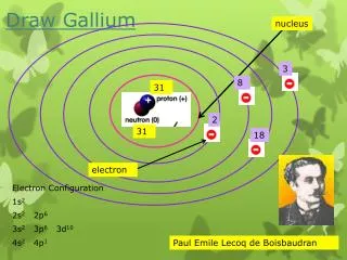
Wait a sec... If GaAs is so superior why is it not everywhere? Gallium is not naturally found in a deposit. Ga diffuses itself into many other substances and is only noticed spectrally or by melting of the substance. This helps explain its relatively late discovery in 1875. An extensive process must be carried out to actually get a “pure” form of Ga. Firstly, one has to melt other materials to find Ga and then once a Ga ingot can be made it must be purified further for semiconductor use, commonly this is performed by zone melting. End result, 99.9999% pure Ga costs ~$15 per gram.
...and... Gallium’s melting point is ~30 C, and as such must be handled in special fashions so that it does not melt and diffuse in its container or surroundings. In its solid phase Ga is actually quite brittle, which again complicates handling. Add to this that GaAs is fairly brittle and wafers are normally limited to about 4” in diameter whereas silicon wafers are typically made at about 12” diameter. This significant decrease in useable area adds again to the expense of a GaAs wafer. Approximate price for a 2” GaAs wafer is ~$100 Whereas a 12” wafer of Si is ~$200
...and... Arsenic itself is a very toxic and needs to be handled delicately to prevent adverse effects (think of Napoleon). Ion implantation has key advantages over diffusion but from a cost and time perspective it is at a severe disadvantage. Although a key property of GaAs is that it has a high electron mobility compared to silicon it has an inferior hole mobility which limits its uses to mainly n-type.