Download
1 / 25
250 likes | 1.1k Vues
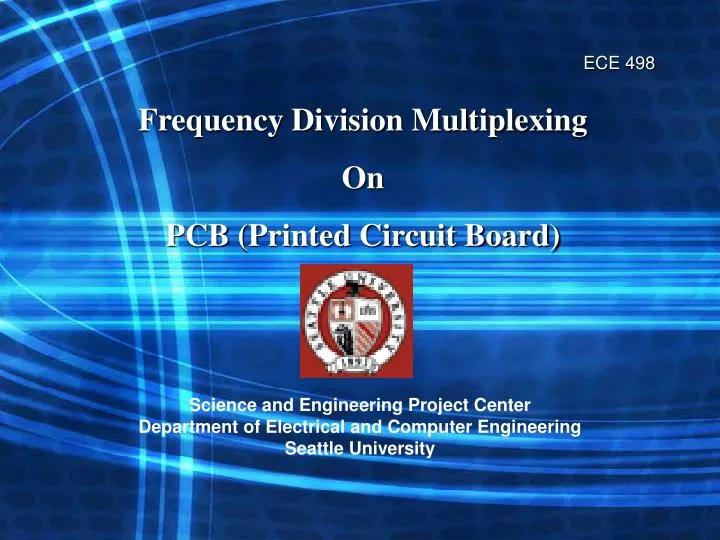
ECE 498 Frequency Division Multiplexing On PCB (Printed Circuit Board) Science and Engineering Project Center Department of Electrical and Computer Engineering Seattle University ECE 498 Frequency Division Multiplexing On PCB (Print Circuit Board) Team Members:

E N D
ECE 498 Frequency Division Multiplexing On PCB (Printed Circuit Board) Science and Engineering Project Center Department of Electrical and Computer Engineering Seattle University
ECE 498 Frequency Division Multiplexing On PCB (Print Circuit Board) Team Members: Kun-Chin Chien Michael Mitchell Faculty Advisor: Dr. Robert G. Heeren Coord. Advisor: Dr. Al Moser
Our Goal • Incorporation of a FDM circuit onto a PCB to allow students to aim their focus on the study of signal flow
Overview • Project Specifics • FDM Laboratory Winter Quarter 05 • Replacement multiplier IC • New PSpice schematic and PCB layout
Project Steps: • Design of Low Pass & Band Pass Filters • Research a PSpice model for the IC and build the complete schematic into PSpice • Research designs for PCB Footprints • Create the Netlist to be imported into OrCad Layout Plus • Design the PCB layout • Route the PCB layout
Analog Devices Analog Multiplier AD633JN
FDM SchematicWith IC AD633JN Adder Modulator Band Pass Filter Demodulator Low Pass Filter
AMP BNC Connector AMP 222132-1
Input 1 Test Point Output 1 +15V Adder Carrier -15V Output 2 Modulator -10V BPF LPF Demodulator 2 Layers Input 2 +10V
Manufactured Price Of the PCB Size of the Board 4.925in(L) X 3.6in(W) Price is dependent on the number of layers, not the number of boards
ECE 498 Conclusion
ECE 498 Questions ????
Thank you for your attention! ECE 498