Download

1 / 37
370 likes | 727 Vues
ECM585 Special Topics in Computer Design Lecture 2. Combinational Logic Design 1 Prof. Taeweon Suh Computer Science Education Korea University Introduction A logic circuit is composed of: Inputs Outputs Functional specification Timing specification Circuits Nodes Inputs: A , B , C

E N D
ECM585Special Topics in Computer DesignLecture 2. Combinational Logic Design 1 Prof. Taeweon Suh Computer Science Education Korea University
Introduction A logic circuit is composed of: • Inputs • Outputs • Functional specification • Timing specification
Circuits • Nodes • Inputs: A, B, C • Outputs: Y, Z • Internal: n1 • Circuit elements • E1, E2, E3
Types of Logic Circuits • Combinational Logic • Memoryless • Outputs determined by current values of inputs • Sequential Logic • Has memory • Outputs determined by previous and current values of inputs
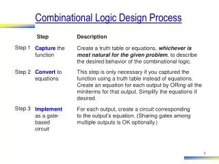
Rules of Combinational Composition • Every circuit element is itself combinational • Every node of the circuit is either designated as an input to the circuit or connects to exactly one output terminal of a circuit element • The circuit contains no cyclic paths: every path through the circuit visits each circuit node at most once • Example:
Boolean Equations • Functional specification of outputs in terms of inputs • Example: S = F(A, B, Cin) Cout = F(A, B, Cin)
Terminology • The Complementof a variable A is A • A variable or its complement is called literal • The AND of one or more literals is called a product orimplicant • Example: AB, ABC, B • OR of one or more literals is called a sum • Example: A + B • Order of operations • NOT has the highest precedence, followed by AND, then OR • Example: Y = A + BC
Sum-of-Products (SOP) Form • All Boolean equations can be written in SOP form • A mintermis a product (AND) of literals involving all of the inputs to the function • Each row in a truth table has a minterm that is TRUE for that row (and only that row) • The function is formed by ORing the minterms for which the output is TRUE • Thus, a sum (OR) of products (AND terms) Y = F(A, B, C) = AB + AB
Product-of-Sums (POS) Form • All Boolean equations can be written in POS form • A maxterm is a sum (OR) of literals • Each row in a truth table has a maxterm that is FALSE for that row (and only that row) • The function is formed by ANDing the maxterms for which the output is FALSE • Thus, a product (AND) of sums (OR terms) Y = F(A, B, C) = (A + B)(A + B)
Boolean Equations Example • You are going to the cafeteria for lunch • You won’t eat lunch (E: eat) • If it’s not open (O: open) • If they only serve corndogs (C: corndogs) • Write a truth table for determining if you will eat lunch (E)
SOP & POS Form • SOP – sum-of-products • POS – product-of-sums Y = AB Y = (A + B)(A + B)(A + B)
When to Use SOP and POS? • SOP produces the shortest equations when the output is true on only a few rows of a truth table • POS is simpler when the output is false on only a few rows of a truth table
HDL • Hardware description language (HDL): allows designer to specify logic function only. Then a computer-aided design (CAD) tool produces the optimized gates. • Most commercial designs built using HDLs • Two leading HDLs: • Verilog • developed in 1984 by Gateway Design Automation • became an IEEE standard (1364) in 1995 • VHDL • Developed in 1981 by the Department of Defense • Became an IEEE standard (1076) in 1987
HDL to Gates • Simulation • Input values are applied to the circuit • Outputs checked for correctness • Millions of dollars saved by debugging in simulation instead of hardware • We are going to use ModelSim Xilinx Edition-III (MXE-III) for simulation • http://www.xilinx.com/ise/optional_prod/mxe.htm • Synthesis • Transforms HDL code into a netlist describing the hardware (i.e., a list of gates and the wires connecting them) • You can see the synthesized result with ISE Webpack IMPORTANT: When describing circuits using an HDL, it’s critical to think of the hardware the code should produce.
Verilog Modules • Two types of Modules: • Behavioral: describe what a module does • Structural: describe how a module is built from simpler modules
Behavioral Verilog Example Verilog: module example(input a, b, c, output y); assign y = ~a & ~b & ~c | a & ~b & ~c | a & ~b & c; endmodule
Behavioral Verilog Simulation Verilog: module example(input a, b, c, output y); assign y = ~a & ~b & ~c | a & ~b & ~c | a & ~b & c; endmodule
Behavioral Verilog Synthesis Verilog: module example(input a, b, c, output y); assign y = ~a & ~b & ~c | a & ~b & ~c | a & ~b & c; endmodule Synthesis:
Verilog Syntax • Verilog is case sensitive. So, reset and Reset are not the same signal. • Verilog does not allow you to start signal or module names with numbers. So, for example, 2mux is an invalid name. • Verilog ignores whitespace. • Comments come in single-line and multi-line varieties: • // single line comment • /* multiline comment */
Structural Modeling - Hierarchy module and3(input a, b, c, output y); assign y = a & b & c; endmodule module inv(input a, output y); assign y = ~a; endmodule module nand3(input a, b, c output y); wire out; // internal signal and3 andgate(a, b, c, out); // instance of and3 inv inverter(out, y); // instance of inverter endmodule
Bitwise Operators module gates(input [3:0] a, b, output [3:0] y1, y2, y3, y4, y5); /* Five different two-input logic gates acting on 4 bit busses */ assign y1 = a & b; // AND assign y2 = a | b; // OR assign y3 = a ^ b; // XOR assign y4 = ~(a & b); // NAND assign y5 = ~(a | b); // NOR endmodule // single line comment /*…*/ multiline comment
Reduction Operators module and8(input [7:0] a, output y); assign y = &a; // &a is much easier to write than // assign y = a[7] & a[6] & a[5] & a[4] & // a[3] & a[2] & a[1] & a[0]; endmodule
Conditional Assignment module mux2(input [3:0] d0, d1, input s, output [3:0] y); assign y = s ? d1 : d0; endmodule ? : is also called a ternary operator because it operates on 3 inputs: s, d1, and d0.
Internal Variables module fulladder(input a, b, cin, output s, cout); wire p, g; // internal nodes assign p = a ^ b; assign g = a & b; assign s = p ^ cin; assign cout = g | (p & cin); endmodule
Precedence Order of operations Highest Lowest
Numbers Format: N'Bvalue N = number of bits, B = base N'B is optional but recommended (default is decimal)
Bit Manipulations: Example 1 assign y = {a[2:1], {3{b[0]}}, a[0], 6’b100_010}; // if y is a 12-bit signal, the above statement produces: y = a[2] a[1] b[0] b[0] b[0] a[0] 1 0 0 0 1 0 // underscores (_) are used for formatting only to make it easier to read. Verilog ignores them.
Bit Manipulations: Example 2 Verilog: module mux2_8(input [7:0] d0, d1, input s, output [7:0] y); mux2 lsbmux(d0[3:0], d1[3:0], s, y[3:0]); // from slide 12 mux2 msbmux(d0[7:4], d1[7:4], s, y[7:4]); // from slide 12 endmodule Synthesis:
Z: Floating Output Verilog: module tristate(input [3:0] a, input en, output [3:0] y); assign y = en ? a : 4'bz; endmodule Synthesis:
Delays module example(input a, b, c, output y); wire ab, bb, cb, n1, n2, n3; assign #1 {ab, bb, cb} = ~{a, b, c}; assign #2 n1 = ab & bb & cb; assign #2 n2 = a & bb & cb; assign #2 n3 = a & bb & c; assign #4 y = n1 | n2 | n3; endmodule
Delays module example(input a, b, c, output y); wire ab, bb, cb, n1, n2, n3; assign #1 {ab, bb, cb} = ~{a, b, c}; assign #2 n1 = ab & bb & cb; assign #2 n2 = a & bb & cb; assign #2 n3 = a & bb & c; assign #4 y = n1 | n2 | n3; endmodule
Testbenches • HDL code written to test another HDL module, the device under test (dut), also called the unit under test (uut) • Not synthesizeable • Types of testbenches: • Simple testbench • Self-checking testbench • Self-checking testbench with testvectors (will be explained later)
Example Write Verilog code to implement the following function in hardware: y = bc + ab Name the module sillyfunction
Example Write Verilog code to implement the following function in hardware: y = bc + ab Name the module sillyfunction Verilog: module sillyfunction(input a, b, c, output y); assign y = ~b & ~c | a & ~b; endmodule
Simple Testbench module testbench1(); reg a, b, c; wire y; // instantiate device under test sillyfunctiondut(a, b, c, y); // apply inputs one at a time initial begin a = 0; b = 0; c = 0; #10; c = 1; #10; b = 1; c = 0; #10; c = 1; #10; a = 1; b = 0; c = 0; #10; c = 1; #10; b = 1; c = 0; #10; c = 1; #10; end endmodule
Self-checking Testbench module testbench2(); reg a, b, c; wire y; // instantiate device under test sillyfunction dut(a, b, c, y); // apply inputs one at a time // checking results initial begin a = 0; b = 0; c = 0; #10; if (y !== 1) $display("000 failed."); c = 1; #10; if (y !== 0) $display("001 failed."); b = 1; c = 0; #10; if (y !== 0) $display("010 failed."); c = 1; #10; if (y !== 0) $display("011 failed.");
Self-checking Testbench (cont.) a = 1; b = 0; c = 0; #10; if (y !== 1) $display("100 failed."); c = 1; #10; if (y !== 1) $display("101 failed."); b = 1; c = 0; #10; if (y !== 0) $display("110 failed."); c = 1; #10; if (y !== 0) $display("111 failed."); end endmodule