Download
1 / 4
40 likes | 98 Vues
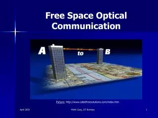
We are communicating with each others for every purpose. Different modes of communication are used. Free space optics is one of the mode of communication. Free space optics is widely used by satellites for transmitting<br>with each other. Design and real prototype fabrication of a low cost portable free space optical transmitter and receiver<br>is presented in this paper. Using this prototype wireless communication is possible. Light from a laser torch is used as<br>the carrier in the circuit. The laser torch can transmit light up to a distance of about 500 meters. The transmitter circuit<br>comprises of condenser microphone transistor amplifier BC548. The gain of the op-amp can be controlled with the help<br>of 1-mega-ohm potmeter. The transmitter uses 9V power supply. The receiver circuit uses an npn phototransistor as<br>the light sensor that is followed by a two-stage transistor preamplifier and LM386-based audio Power amplifier. This<br>paper deals with the designing of a very low cost free space optical system which is perfect for information<br>transmission of general conversation, using an ordinary available Laser torch of cost. The circuit is designed using<br>National Instrumentations Multisim11.0 (N.I. Multisim 11.0) and National Instrumentations UltiBoard11.0 (N.I.<br>UltiBoard 11.0).

E N D
ISSN (Online) : 2278-1021 ISSN (Print) : 2319-5940 International Journal of Advanced Research in Computer and Communication Engineering Vol. 3, Issue 6, June 2014 Design and Real Prototype Fabrication Of a Free Space Optical Transmitter and Receiver S.Srinath UG Student, ECE, Vellore Institute of Technology, Vellore, India Abstract:We are communicating with each others for every purpose. Different modes of communication are used. Free space optics is one of the mode of communication. Free space optics is widely used by satellites for transmitting with each other. Design and real prototype fabrication of a low cost portable free space optical transmitter and receiver is presented in this paper. Using this prototype wireless communication is possible. Light from a laser torch is used as the carrier in the circuit. The laser torch can transmit light up to a distance of about 500 meters. The transmitter circuit comprises of condenser microphone transistor amplifier BC548. The gain of the op-amp can be controlled with the help of 1-mega-ohm potmeter. The transmitter uses 9V power supply. The receiver circuit uses an npn phototransistor as the light sensor that is followed by a two-stage transistor preamplifier and LM386-based audio Power amplifier. This paper deals with the designing of a very low cost free space optical system which is perfect for information transmission of general conversation, using an ordinary available Laser torch of cost. The circuit is designed using National Instrumentations Multisim11.0 (N.I. Multisim 11.0) and National Instrumentations UltiBoard11.0 (N.I. UltiBoard 11.0). Keywords: Battery driven design, Free space optics, Laser torch, Low cost design, N.I. Multisim and N.I. UltiBoard Simulator, Voice or data transmission. I. INTRODUCTION This paper is based on the concept of Laser (Light Amplification by Stimulated Emission of Radiation) for transmitting analog as well as digital signals. As laser is stimulated radiation, problem of interference occurs in electromagnetic wave is eliminated, it can be a good substitution of present day communication systems and high deal of secrecy is available. Use of laser in communication systems is the future because of the advantages of the full channel speeds, no communication licenses required at present, compatibility with copper or fiber interfaces and no bridge or router requirements. Also it cannot be detected with use of spectrum analyzers and RF meters and hence can be used for diverse applications including financial, medical and military. Lasers can also transmit through glass. Laser transmitter and receiver units ensure easy, straightforward systems alignment and long- term stable, service free operation, especially in inaccessible environments. Optical wireless systems offer ideal, economical alternative to expensive leased lines for buildings. The laser can be commissioned in satellites for communication, as laser radar requires small aperture as compared to microwave radar. For voice transmission amplitude modulation of laser pulse was used to transmit the voice signal. Condenser microphone converts the voice into electric pulse which was then amplified and transmitted through laser. Photo detector at receiver detects the laser light and voice was output through loud speaker. II. RELATEDWORK This paper presents the design and real prototype fabrication of a free space optical system. The circuits are simulated in N.I. Multisim 11.0 and checked for validity and routing for the P.C.B. design is done with N.I. UltiBoard 11.0. The given design is thus checked and routed as per „INDUSTRY STANDARDS‟ and the real prototype can thus be etched out and a P.C.B. can be made on which components can be easily soldered. This paper mainly focuses on checking the validity of my design and performing a routing for my design for making a P.C.B. III. OBJECTIVESOFTHEDESIGN This paper aims to provide simple and cheap wireless communication design and real prototype fabrication for larger date rate with less distortion and to reduce the complexity for communication in the places where optical fiber or any wired communication is very difficult and expensive. The design is so easy, inexpensive and makeable with the available equipments that the technical as well as non technical person can construct it by themselves for their personal use. A. Block Diagram and Algorithm used for the Design Fig. 1 Block Diagram for Voice and Data Transmission The algorithm is as follows. The input voice is taken through condenser microphone or a plug-in is taken as the input. The voice signal is amplified through the 7268 Copyright to IJARCCE www.ijarcce.com
ISSN (Online) : 2278-1021 ISSN (Print) : 2319-5940 preamplifier phase. Then, the signal is transmitted through laser light. The phototransistor at receiving side converts the signal into electrical signal. The electrical signal is passed through two transistor amplifier phases. Then LM386 audio amplifier amplifies the signal and drive speaker to generate voice output. Flow Chart for Transmitter Circuit : Flow Chart for Receiver Circuit : IV. EQUIPMENTSREQUIRED TABLEI EQUIPMENTSREQUIRED Resistors All of (1/4)W, 5% unless otherwise stated International Journal of Advanced Research in Computer and Communication Engineering Vol. 3, Issue 6, June 2014 10K (brown, black, orange) 1Num BC547 transistor 1 Num. IF-D93 detector (red dot on black case) 1Num IF-E96 emitter (pink dot on blue case) 1Num Electret Microphone 1Num 10 nF mylar (103) 2 Nos. 22K (red, red, orange) 2 Nos. 47nF box poly 1 Num 100K (brown, black, yellow) 4Nos - Start 220K (red, red, yellow) 1 Num. 680K (blue, grey, yellow) 1Num. 1M (brown, black, green) 1Num. 100K Koa trimpot (104) 1Num. - Get input from user Speaker 8 ohm, 1W 1Num - Pre –Amplifier Stage 8 pin DIL IC socket 3 Nos. - Modulation and Tx of Signal 2 pole terminal block 3Nos. - 9V battery snap 2Nos. - - Photo-Transistor Circuit for Detection V. WORKINGOFCIRCUITDIAGRAMOF TRANSMITTER The electret microphone converts sound waves to an electrical signal in the Tx circuit. R1 provides DC bias for the microphone and should be removed if you wish to connect any other input instead. This signal is coupled via C2 and amplified by two LM358 op amps, and converted to an optical signal by the LED emitter, driven from transistor Q1. R3 and R6 set the gain of IC1A to 1+R3/R6, or 221. Since IC1A is direct coupled, R4/R2 determine the DC input and thus the DC output level. IC1B is also direct coupled and provides both the DC base current for Q1 and the AC modulation current. R7 determines the DC bias current for Q1. The modulated collector current drives the LED emitter. De-Modulation of Voice or Data Output to Loudspeaker Stop Capacitors Others 10R (brown, black, black) 1 Num 100 uF electrolytic 1Num LM 358 IC 2Nos Fig. 2 Transmitter schematic in N.I. Multisim 11.0 VI. REALPROTOTYPEFABRICATIONOF TRANSMITTER After checking the validity of the circuit in N.I. Multisim11.0, now convert the circuit to UltiBoard 11.0. To do this check if all the components are blue in colour(i.e. they have a foot-print) and select „Transfer To UltiBoard 11.0‟ button. 100R (brown, black, brown) 2 Num. 1K (brown, black, red) 1Num 10 uF electrolytic 3Nos. 100 nF monoblock (104) 4 Nos. LM 386 IC 1Num. 78L05 regulator 1Num 7269 Copyright to IJARCCE www.ijarcce.com
ISSN (Online) : 2278-1021 ISSN (Print) : 2319-5940 International Journal of Advanced Research in Computer and Communication Engineering Vol. 3, Issue 6, June 2014 VII. WORKINGOFCIRCUITDIAGRAMOF RECEIVER At the other end of the cable, the optical signal is directed at a photo-darlington detector in the receiver that converts it into an electrical signal again. The signal is amplified by op amp IC2 and power amp IC3 before being fed into a speaker where it becomes a sound wave. A voltage regulator has been used in the receiver gain stage to reduce DC supply ripple caused by the higher currents drawn in the power amplifier section. C1 and C2 are filter caps, C3 couples the detector voltage imposed across R1, into IC2. R2 and R4 set the op amp input to half the supply voltage, since only one supply is used rather than positive and negative supplies, as is usually the case. The gain of IC2 is adjustable by the pot in the feedback circuit. The range is therefore 1+1M/110k to 1+1M/10k, or 10 to 101. This is used as a volume control. IC2 output is coupled via C6 into an LM386 power amp IC with gain set to 20. R6 and C8 act as a low pass filter on the input. R7 and C9 form a network that provides a high frequency load to ensure stability. Fig. 3 Basic View of the Converted Schematic in N.I. UltiBoard 11.0 Now, align the components on the workspace and perform „Routing‟. Fig. 4 View after Performing Routing of the Schematic in N.I. UltiBoard 11.0 for Transmitter Design The 3D View of the real prototype fabrication of my design is shown below. Fig. 7 Receiver schematic in N.I. Multisim 11.0 VIII. REALPROTOTYPEFABRICATIONOF RECEIVER After checking the validity of the circuit in N.I. Multisim11.0, now convert the circuit to UltiBoard 11.0. To do this check if all the components are blue in colour(i.e. they have a foot-print) and select „Transfer To UltiBoard 11.0‟ button. Fig. 5 3D View of my Design Showing PCB Connections for Transmitter Design Fig. 8 View after Performing Routing of the Schematic in N.I. UltiBoard 11.0 for Receiver Design The 3D View of the real prototype fabrication of my design is shown below. Fig. 6 3D View Showing Connections Appearing at the back-side of the PCB for Transmitter Design 7270 Copyright to IJARCCE www.ijarcce.com
ISSN (Online) : 2278-1021 ISSN (Print) : 2319-5940 International Journal of Advanced Research in Computer and Communication Engineering Vol. 3, Issue 6, June 2014 and Reception are cheaper and simpler in construction than RF transmitter and receiver. Although, wireless communication predominantly means the use of radio frequency for communication, the use of light based carriers for transfer of information is explored in this paper. This design can be made and used successfully at political assembly, lecture halls and for general conversation between two houses. The main problem with lasers is the beam dispersion can occurs due to external factors. In order to overcome these problems most advanced powerful lasers are to be employed.Although the optical data communication technology is prevailing from last decade as optical fiber communication devices available in the market, this design was presented to get all ideas that are behind such wireless system. ACKNOWLEDGMENT At the outset, I would like to express my gratitude for my institute – Vellore Institute of Technology (V.I.T.) for providing me with the opportunity to undergo my undergraduate training, and assimilate knowledge and experience hitherto unknown to me. REFERENCES [1]I. Melngailis, “Laser development in Lincoln laboratory”, The Lincoln Laboratory Journal, vol. 3, no. 3, pp. 347, 1990. [2]I. R. Sinclair and J. Dunton, “Practical Electronics Handbook”, 6thed. Oxford, U.K, Newnes, 2007, pp. 252-255. [3]Sedra, Adel.S and Smith, Kenneth C, “Microelectronic Circuits”, Oxford University Press, 1998. [4]T. L. Floyd, “Electronic Devices”, 6th ed. Singapore, Pearson Education, 2002, pp. 559-561. [5]C. M. M. Paschoal, D. Do N. Souza, and L. A. P. Santo, “Characterization of three photo detector types for computed tomography dosimetry”, World Academy of Science, Engineering and Technology, no. 56, pp. 92-95, August 2011 [6]“Laser and its applications,” Popular Science & Technology Series, DRDO Publications, 2009. [7]O. Bishop, “Electronics Circuits and Systems”, 4th ed. Oxford, U.K, Newnes, 2011, pp. 14. [8]I. R. Sinclair and J. Dunton, “Practical Electronics Handbook”, 6th ed. Oxford, U.K, Newnes, 2007, pp. 252-255. [9]M. S. Islam and M. A. Rahman, “Design and fabrication of line follower robot,” Asian Journal of Applied Science and Engineering, vol. 2, no. 2, pp. 27-32, 2013. [10]W. Tomasi, “Advanced Electronic Communication System”, 6th ed.. New Jersey, U.S.A, Prentice-Hall, 2004, pp. 3, 41-42. [11]S. Gibilisco, “The Illustrated Dictionary of Electronics”, 8th ed. New York, U.S.A, McGraw-Hill, 2001, pp. 399. [12]S. C. Singh, H. B. Zeng, C. L. Guo, and W. P. Cai, “Nanomaterials: Processing and Characterization with Lasers”, 1sted. Wiley-VCH Verlag GmbH & Co. KGaA., 2012, ch. 1, pp.1. BIOGRAPHY S.SRINATH passed 10th C.B.S.E. Board with a mark of 475/500(95%) and 12th C.B.S.E. Board from D.A.V. Boys Senior Gopalpuram, Chennai with a mark of 458/500(91.6%).Currently studying B.Tech, ECE, School of Electronics Engineering in VIT University, Vellore, India. Fig. 9 3D View of my Design Showing PCB Connections for Receiver Design Fig. 10 3D Side View of my Design Showing PCB Connections for Receiver Design Fig. 11 3D View Showing Connections Appearing at the back-side of the PCB for Receiver Design IX. ADVANTAGES Light from a laser torch is used as the carrier in the circuit instead of RF and FM signals. The laser transmission is very secure because it has a narrow beam[6]. The main advantage of this system is high reliability as it is impossible to track the data on the way of transmission. This design of Laser voice transmission system can be made at anywhere with low cost and can be used for frequent conversation at free of cost instead of using cell phone. X. CONCLUSION This paper is completely based on wireless communication system. Presently there are various techniques which are being successfully used for transmission of data. The data transmission techniques employ RF, FM signals for transmission of data. Laser Torch Based Transmission Secondary School, he is 7271 Copyright to IJARCCE www.ijarcce.com