Download
1 / 1
20 likes | 144 Vues
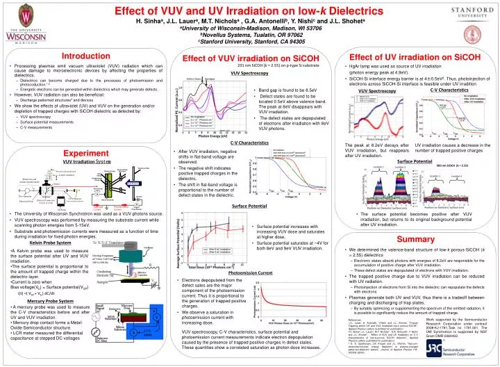
Effect of VUV and UV Irradiation on low- k Dielectrics. H. Sinha a , J.L. Lauer a , M.T. Nichols a , G.A. Antonelli b , Y. Nishi c and J.L. Shohet a a University of Wisconsin-Madison, Madison, WI 53706 b Novellus Systems, Tualatin, OR 97062 c Stanford University, Stanford, CA 94305.

E N D
Effect of VUV and UV Irradiation on low-kDielectrics • H. Sinhaa, J.L. Lauera, M.T. Nicholsa , G.A. Antonellib, Y. Nishic and J.L. Shoheta • aUniversity of Wisconsin-Madison, Madison, WI 53706 • bNovellus Systems, Tualatin, OR 97062 • cStanford University, Stanford, CA 94305 Introduction Effect of VUV irradiation on SiCOH Effect of UV irradiation on SiCOH 231 nm SiCOH (k = 2.55) on p-type Si substrate • HgAr lamp was used as source of UV irradiation • (photon energy peak at 4.9eV). • SiCOH-Si interface energy barrier is at 4±0.5eV2. Thus, photoinjection of electrons across SiCOH-Si interface is feasible under UV irradition • Processing plasmas emit vacuum ultraviolet (VUV) radiation which can cause damage to microelectronic devices by affecting the properties of dielectrics. • Dielectrics can become charged due to the processes of photoemission and photocoduction.1,2 • Energetic electrons can be generated within dielectrics which may generate defects. • However, VUV radiation can also be beneficial: • Discharge patterned structures3 and devices • We show the effects of ultraviolet (UV) and VUV on the generation and/or depletion of trapped charges with SiCOH dielectric asdetected by: • VUV spectroscopy • Surface potential measurements • C-V measurements VUV Spectroscopy • Band gap is found to be 8.5eV • Defect states are found to be located 0.5eV above valence band. The peak at 8eV disappears with VUV irradiation. • The defect states are depopulated of electrons after irradiation with 8eV VUV photons. C-V Characteristics VUV Spectroscopy C-V Characteristics The peak at 8.2eV decays after VUV irradiation, but reappears after UV irradiation. UV irradiation causes a decrease in the number of trapped positive charges Experiment • After VUV irradiation, negative shifts in flat-band voltage are observed. • The negative shift indicates positive trapped charges in the dielectric. • The shift in flat-band voltage is proportional to the number of defect states in the dielectric. VUV Irradiation System Surface Potential 500 nm SiOCH (k = 2.55) Surface Potential • The University of Wisconsin Synchrotron was used as a VUV photons source. • VUV spectroscopy was performed by measuring the substrate current while scanning photon energies from 5-15eV. • Substrate and photoemission currents were measured as a function of time during irradiation for fixed photon energies. • The surface potential becomes positive after VUV irradiation, but returns to its original background potential after UV irradiation. • Surface potential increases with increasing VUV dose and saturates at higher dose. • Surface potential saturates at ~4V for both 8eV and 9eV VUV irradiation. Summary Kelvin Probe System • We determined the valence-band structure of low-k porous-SiCOH (k = 2.55) dielectrics • Electronic states absorb photons with energies of 8.2eV are responsible for the accumulation of positive charge after VUV irradiation. • These defect states are depopulated of electrons with VUV irradiation. • The trapped positive charge due to VUV irradiation can be reduced with UV radiation. • Photoinjection of electrons from Si into the dielectric can repopulate the defects with electrons • Plasmas generate both UV and VUV, thus there is a tradeoff between charging and discharging of trap states. • By suitably optimizing or supplementing the spectrum of the emitted radiation, it is possible to significantly reduce the amount of trapped charge. • A Kelvin probe was used to measure the surface potential after UV and VUV irradiation. • The surface potential is proportional to the amount of trapped charge within the dielectric layer. • Current is zero when • Bias voltage(Vb) = Surface potential(VSP) Photoemission Current • Electrons depopulated from the defect sates are the major component of the photoemission current. Thus it is proportional to the generation of trapped positive charges. • We observe a saturation in photoemission current with increasing dose. C i(t) =( VSP + Vb ) dC/dt Mercury Probe System • A mercury probe was used to measure the C-V characteristics before and after UV and VUV irradiation. • Mercury drop contact forms a Metal-Oxide-Semiconductor structure. • LCR meter measured the differential capacitance at stepped DC voltages Work supported by the Semiconductor Research Corporation under contract 2008-KJ-1781,Task no 1781.001. The UW Synchrotron is supported by NSF Grant DMR-0084402. • References: • 1J.L. Lauer, A. Antonelli, Y.Nishi and J.L. Shohet, "Charge Trapping within UV and VUV Irradiated low-k porous-SiCOH", Applied Physics Letters (submitted for publication) • 2 H. Sinhaa, J.L. Lauera, M.T. Nicholsa , G.A. Antonellib, Y. Nishic and J.L. Shoheta , “Effect of VUV and UV Irradiation on C-V characteristics of low-k-porous SiCOH dielectric”, Applied Physics Letters (submitted for publication) • 3 G. S. Upadhyaya, J.B. Kruger and J.L. Shohet, "Vacuum-ultraviolet-induced charge depletion in plasma-charged patterned-dielectric wafers", Journal of Applied Physics 105, 053308 (2009). VUV spectroscopy, C-V characteristics, surface potential and photoemission current measurements indicate electron depopulation caused by the presence of trapped positive charges in defect states. These quantities show a correlated saturation as photon dose increases.