Download
1 / 24
250 likes | 505 Vues
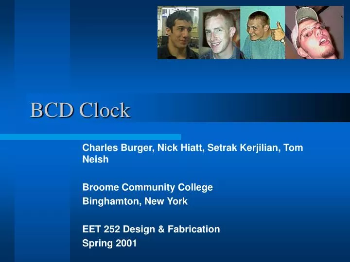
BCD Clock. Charles Burger, Nick Hiatt, Setrak Kerjilian, Tom Neish Broome Community College Binghamton, New York EET 252 Design & Fabrication Spring 2001. Project Goals. Computer Driven Binary Clock Marketable Small, Attractive Product Low Cost Production.

E N D
BCD Clock Charles Burger, Nick Hiatt, Setrak Kerjilian, Tom Neish Broome Community College Binghamton, New York EET 252 Design & Fabrication Spring 2001
Project Goals • Computer Driven Binary Clock • Marketable • Small, Attractive Product • Low Cost Production
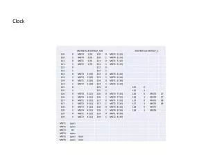
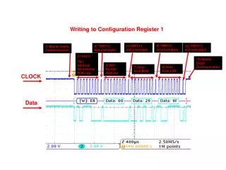
Heart of the Circuit - 74LS595 IC 8 Bit Shift Register with Output Latches • 8 Shift Registers • 8 Latches
Heart of the Circuit - 74LS595 IC Shift Registers • Row of cascaded flip-flops (21 bits required) • Serial Input • Parallel Output to Latches • Shifted by Clock
Heart of the Circuit - 74LS595 IC • Latches • Sustains high or low value from Shift Register • Triggered by RCK Input • Outputs and Drives LED’s
Other Electrical Components • Resistors • Purpose: To act as Current Limiting Device • Light Emitting Diodes • Visual Output Display
Circuit Design • Circuit Design • One Chip for each digit (hrs., min., sec.) • Off-board Connector Location • Minimize Traces • Minimize PCB size
Circuit Design • Breadboard Circuit Check Why Breadboard First?
Printed Circuit Board Design • Design Rules • Trace and Pad Spacing • Dead Space • Component Spacing • Placement of Components
Pre-Fabrication Requirements • Circuit Check • Parts List • Jumper Pin-Out • Drill Plan
Pre-Fabrication Requirements Circuit Check • Why do a Circuit Check? • Ensure that Schematic and PCB Design match electrically. • Future Troubleshooting Aid
Pre-Fabrication Requirements Parts List • Cost Assessment • Manufacture Preparation • Repair Information
Pre-Fabrication Requirements Jumper Pin-Out • Assembly Aid • Troubleshooting Aid
Pre-Fabrication Requirements Drill Plan Assembly Aid • Necessary Hardware • Drilling Location
Fabrication • Fabrication of Printed Circuit Board • Fabrication of Chassis • Fabrication of Cover
Mylar PhotoResist Mylar and Copper Exposed to UV Light Heat Treatment Removal of Exposed Photo Resist Etching of PCB Removed Remaining PhotoResist Drilled Holes Tinned Traces Trimmed PCB Filed Edges LED Spacer Fabrication of PCB
Fabrication of PCB • Insertion and Fitting of Components • Lead Soldering • De-Fluxing • Functionality Test
Fabrication of Chassis • Chose Appropriate Size Aluminum Box • Drilled Holes for DB-9, PBC Mounts, and Cover • Applied Paint
Fabrication of Cover • Choice of Cover • Aesthetically Pleasing • Colorful • Testing of Cover • Manufacture • Cut plexiglass to size • Drilled holes for LEDs • Drilled Mounting Holes • Engraved Lettering
Special Thanks To: Don McCarty Mr. Antanakos and of course, Mr. DiGiacomo Mr. De Voe