Download

1 / 15
150 likes | 306 Vues
Low energy X-Ray Spectroscopic Applications of Very Large Area Silicon Drift Detector. ABSTRACT

E N D
Low energy X-Ray SpectroscopicApplications of Very Large AreaSilicon Drift Detector ABSTRACT The spectroscopic performances of a very large sensitive area SDD (about 53 cm2) at the energies of 241Am and 55Fe sources shows that the goal of a high energy resolution combined with large sensitive areas can be achieved. This result has moved a large interest and the present project proposes a further development of this detectors in the direction of high performances x ray spectroscopy. Andrea Vacchi Infn Trieste
INFN Trieste laboratories Silicon Drift Detectors from device modeling to mass production - practical experience • From specs to detector • HV divider & stability • Injectors & drift speed variations • NTD fluctuations • Safe design & yield • Radiation damage • Mass production SDD first proposed by E. Gatti P. Rehak 1984 Andrea Vacchi Infn Trieste
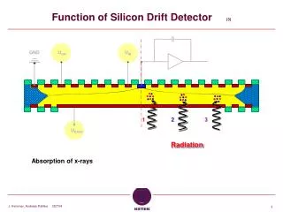
divider metal anodes depletion potential -U n-side p-side oxide (SiO2) drift potential anode drift distance Silicon drift detectors (SDD) • due to their collection electrode geometry, SDD haveexcellent noise performance and are well suited for low-energy X-ray spectroscopy applications. By means of a series of cathodes (biased with a scaling potential) a highly-linear drift field is established from the center of the detector towards two arrays of anodes placed at opposite sides of the SDD. Andrea Vacchi Infn Trieste
The silicon drift detector (SDD) This design of this SDD originates from the primary need to perform unambiguous measurement of the impact point of charged particles along both the X and Y axis in presence of high multiplicity, together with a large sensitive area. The ionizing radiation create electron-hole pairs: the electron cloud is focused at the center of the silicon bulk and drifts to the anodes, while the holes are collected by the cathodes. When the electrons reach the end of the drift zone, they are abruptly pushed towards the anodes by an electrode (placed beneath them) in order to minimize the collecting time. The X coordinate is measured along the anodes where the charge is collected, the Y coordinate corresponds to the travel time of the electrons. Ionising radiation anode electrons Simulation of the potential distribution in the SDD Andrea Vacchi Infn Trieste
256 readout anodes drift 256 readout anodes The SDD was selected to equip the 3rd and 4th layers of the Inner Tracking System (ITS) of the ALICE experiment at LHC. The finger print of this silicon drift detector is: 256 readout anodes 256 readout anodes drift drift drift • Wafer type: • 5” Neutron Transmutation Doped <111> 3 k.cm, 300 m thick • Area: • sensitive: 7.02 7.53 cm2, divided into two drift regions • total: 7.25 8.76 cm2, (ratio = 0.83) • Each drift region: • 35 mm long • 291 cathodes driven by built-in voltage divider • 256 anodes – 294 m pitch • 3 rows of 33 MOS charge injectors (for the drift velocity calibration) • Guard regions: • independent built-in voltage dividers 256 readout anodes 256 readout anodes 256 readout anodes 256 readout anodes 256 readout anodes Typical operating parameters: • Drift bias voltage: -2.4 kV, 8V/cathode E=670V/cm • Maximum drift time : 4.3 s, vd =8 m/ns • Power dissipation on board:0.95 W • equivalent Rtot of all drift + guard dividers 4781 kΩ • total current in all dividers ~0.40 mA Andrea Vacchi Infn Trieste
Detector design features integrated dividers generate the biases for all of the drift cathodes and the guard region which used to scale down gradually the negative high-voltage to ground at the edge of the SDD. sets of MOS injectors placed at different distances from the anodes are used for the drift velocity calibration. injector lines close-up injector line bonding pad MOS injector (every 8th anode) collection zone close-up guard cathodes (32 mm pitch) 292 drift cathodes (120 mm pitch) implanted HV voltage dividers 256 collection anodes (294 mm pitch) Andrea Vacchi Infn Trieste
anode axis (Z) • drift-time axis (R-F) Resolution (mm) Drift distance (mm) About 600 detectors have been produced using a dedicated double sided process. Due to the redundant design and production technology the yield was grater than 60% . 260 detectors (84 in layer 3 and 176 in layer 4) have been mounted on the barrel of the ALICE-ITS now in the commissioning phase acquiring cosmic muons data. reconstruct the impact position of the ionizing particles with a resolution better than 30µm in both X and Y axis. Beam-test data Andrea Vacchi Infn Trieste
suitable for low-energy X-ray spectroscopy applications: + anode capacitance is about 50 fF, + the leakage current at the anode measured at room temperature is very low This allows a very-low noise contribution from the front-end electronics. Considering its sensitive area, more than an order of magnitude larger than that of the standard SDDs, this detector could open the way to application areas of the X-ray spectroscopy that require wide surface coverage. Each anode sees a 10 mm2 surface - the reported current values correspond to 4 anodes read-out together Andrea Vacchi Infn Trieste
Bias board The measurement setup Climatic chamber The detector and the front-end electronics are placed in a climatic chamber able to control the temperature. This also acts as shield detector and electronics from irradiated noise. Andrea Vacchi Infn Trieste
Bias board Detector board RADIOACTIVE SOURCE BIAS CONNECTOR COLLIMATOR JFETs TO PREAMPLIFIERS The last 6 drift cathodes near the anodes are decoupled directly on the detector board to minimize noise coupling. An aluminum block is used to collimate the radioactive source. This minimizes the partial charge collection. The collimator, 4cm high, has a thin slit (about 0.5mm) that allows to illuminate almost the whole drift length of a set of anodes. It sits 5mm above the detector. A low capacitance JFET (CGS = 0.4pF) is connected to a group of 4 anodes (CDet,tot = 0.2pF) and read out by a multi-channel preamplifier board. The JFET integrates a feedback capacitor CF = 50fF, and a transistor to discharge the capacitor realizing the reset of the preamplifier. The total capacitance measured at the input of the preamplifier (the gate of the JFET) is about 1pF Andrea Vacchi Infn Trieste
Counts 560 eV FWHM @ 13.95keV 4% ADC channels 241Am spectrum measured at +16°C with a trapezoidal shaping having a rise/fall time tR = 0.4µs and a flat top of 0.2µs. The high voltage bias of the detector is -1600V. The leakage current of the four anodes is ~ 5pA Andrea Vacchi Infn Trieste
Counts Mn kα 386 eV FWHM 7% Mn kβ ADC channels 55Fe spectrum measured at 0°C with a trapezoidal shaping having a rise/fall time tR = 1.2µs and a flat top of 0.2µs. The high voltage bias of the detector is -1300V. The leakage current of the four anodes is ~ 1pA. The red line represents the fit function used to determine the energy resolution. Andrea Vacchi Infn Trieste
Next step on board first stageDetail fet F2 for Andrea Vacchi Infn Trieste
Participants: • - Isaf Roma • Marco Feroci • Ictp Trieste • Dipak Debnath • Debashis Bhowmick • Ritabrata Sarkar • Claudio Tuniz • Andres Cicuttin • Mliz Crespo • - Infn Trieste • Gianluigi Zampa • Andrea Vacchi • Alexandre Rashevsky • Valter Bonvicini • Erik Vallazza • - Iasf Bologna • Labanti • - Infn Bologna • Giuseppe Baldazzi • - PoliMilano • Longoni • - Concluding • Largest drift detector • Active area: 52 cm2 • Anode pitch: 294µm • 512 anodes on two rows • Position resolution: <50µm • MOS injectors for calibration • Targets: • High-resolution low noise large area silicon detectors based on the Silicon Drift Detector principle. • o Low energy X-ray spectroscopy • o Radioactivity contamination detectors • o Atomic physics studies • o X - ray astronomy • o Medical applications Andrea Vacchi Infn Trieste