Download
1 / 27
270 likes | 395 Vues
SLAAC Register Definitions Release 2.0. Register # Name SLAAC-1- specific? 0 ENABLE Y 1 2 REVISION0 Y 3 REVISION1 Y 4 CONF_PROG 5 CONF_DATA 6 CONF_DONE 7 8 RB_TRIG 9 RB_START 10 RB_END 11 12 EEPROM_START 13 EEPROM_CLOCK 14 EEPROM_DATA 15 EEPROM_PROG 16 HDSK_EN 17 HDSK_X0

E N D
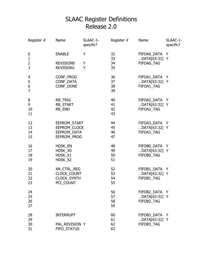
SLAAC Register Definitions Release 2.0 Register # Name SLAAC-1- specific? 0 ENABLE Y 1 2 REVISION0 Y 3 REVISION1 Y 4 CONF_PROG 5 CONF_DATA 6 CONF_DONE 7 8 RB_TRIG 9 RB_START 10 RB_END 11 12 EEPROM_START 13 EEPROM_CLOCK 14 EEPROM_DATA 15 EEPROM_PROG 16 HDSK_EN 17 HDSK_X0 18 HDSK_X1 19 HDSK_X2 20 XN_CTRL_REG 21 CLOCK_COUNT 22 CLOCK_SYNTH 23 PCI_COUNT 24 25 26 27 28 INTERRUPT 29 30 PAL_REVISION Y 31 FIFO_STATUS Register # Name SLAAC-1- specific? 32 FIFOA0_DATA Y 33 …DATA[63:32] Y 34 FIFOA0_TAG 35 36 FIFOA1_DATA Y 37 …DATA[63:32] Y 38 FIFOA1_TAG 39 40 FIFOA2_DATA Y 41 …DATA[63:32] Y 42 FIFOA2_TAG 43 44 FIFOA3_DATA Y 45 …DATA[63:32] Y 46 FIFOA3_TAG 47 48 FIFOB0_DATA Y 49 …DATA[63:32] Y 50 FIFOB0_TAG 51 52 FIFOB1_DATA Y 53 …DATA[63:32] Y 54 FIFOB1_TAG 55 56 FIFOB2_DATA Y 57 …DATA[63:32] Y 58 FIFOB2_TAG 59 60 FIFOB3_DATA Y 61 …DATA[63:32] Y 62 FIFOB3_TAG 63
fifo hdsk synth config eeprom interrupt readback xn_ctrl_reg fifo_loopback ext_mem_bus led_mode[1:0] pwr_monitor_status Register #0: ENABLE_STATUS String lookup: “enable” Class member: Slaac1Board::EnableStatus status enable 31 30 29 28 27 26 25 24 23 22 21 20 19 18 17 16 15 14 13 12 11 10 9 8 7 6 5 4 3 2 1 0 reserved reserved Function: Contains the enable bits for IF functional blocks and the core IF status bits. Note that it is a good idea to disable blocks that are not in use, because some blocks re-use I/O pins that have different purposes in normal execution (main example is the configuration module). Bitfields: led_mode: “00” (reset state) causes the all IF LEDs to light up; “10” (written by driver) causes IF LEDs to display a counter These bits are enables for the following IF functional blocks: config: configuration module synth: clock synthesizer control xn_ctrl_reg: the FPGA control register ext_mem_bus: the external memory bus fifo: the FIFOs fifo_loopback: “loopback” (debug) mode for the FIFOs readback: the readback controller eeprom: the eeprom controller hdsk: the handshake registers interrupt: the interrupt module pwr_monitor_status: Set to ‘0’ by current monitor if current threshold is exceeded
day[4:0] hour[4:0] month[3:0] year_bottom[5:0] Register #2: REVISION0 String lookup: “revision0” Class member: Slaac1Board::Revision0 Special notes: Read-only 31 30 29 28 27 26 25 24 23 22 21 20 19 18 17 16 15 14 13 12 11 10 9 8 7 6 5 4 3 2 1 0 minute[5:0] second[5:0] Function: Contains the bottom 32 bits of IF revision data. The bitfields in this register indicate the date and time the IF configuration was compiled. The year field is split across REVISION0 and REVISION1. Bitfields: second minute hour day month year_bottom: Bottom 6 bits of the year field; top 8 bits are contained in REVISION1 (yes we are Y2K compliant!)
Register #3: REVISION1 String lookup: “revision1” Class member: Slaac1Board::Revision1 Special notes: Read-only 31 30 29 28 27 26 25 24 23 22 21 20 19 18 17 16 15 14 13 12 11 10 9 8 7 6 5 4 3 2 1 0 minor[7:0] major[7:0] year_top[7:0] subminor[7:0] Function: Contains the top 32 bits of IF revision data. The bitfields in this register indicate the assigned release number (major.minor.subminor), plus the top 8 bits of the year field as continued from REVISION0. Bitfields: year_top: Top 8 bits of the year field; bottom 6 bits are contained in REVISION0 (yes we are Y2K compliant!) subminor minor major
x2 x1 x0 Register #4: CONF_PROG String lookup: “conf_prog” Class member: SlaacBoard::ConfProg 31 30 29 28 27 26 25 24 23 22 21 20 19 18 17 16 15 14 13 12 11 10 9 8 7 6 5 4 3 2 1 0 reserved Function: Controls the PROGRAM_N pins of the PEs, which are used to initiate configuration. These signals are low-asserted, i.e. a ‘0’ on these signals clear the configuration of the corresponding PE. Bitfields: x0: The PROGRAM_N pin of PE X0 x1: The PROGRAM_N pin of PE X1 x2: The PROGRAM_N pin of PE X2
x2 x1 x0 Register #5: CONF_DATA String lookup: “conf_data” Class member: SlaacBoard::ConfData 31 30 29 28 27 26 25 24 23 22 21 20 19 18 17 16 15 14 13 12 11 10 9 8 7 6 5 4 3 2 1 0 reserved Function: Controls the DIN pins of the PEs, which are used to shift in serial configuration data. Note that these pins are re-used by the PEs after configuration. Therefore it is essential to disable the configuration module in order to return these signals to their default (non-configuration) modes. Bitfields: x0: The DIN pin of PE X0 x1: The DIN pin of PE X1 x2: The DIN pin of PE X2
x2 x1 x0 Register #6: CONF_DONE String lookup: “conf_done” Class member: SlaacBoard::ConfDone Special notes: Read-only 31 30 29 28 27 26 25 24 23 22 21 20 19 18 17 16 15 14 13 12 11 10 9 8 7 6 5 4 3 2 1 0 reserved Function: Reads the DONE pins of the PEs, which are used to signal successful completion of configuration. A PE is configured when its DONE pin is high-asserted. Bitfields: x0: The DONE pin of PE X0 x1: The DONE pin of PE X1 x2: The DONE pin of PE X2
x2 x1 x0 busy Register #8: RB_TRIG String lookup: “rb_trig” Class member: SlaacBoard::RBTrig 31 30 29 28 27 26 25 24 23 22 21 20 19 18 17 16 15 14 13 12 11 10 9 8 7 6 5 4 3 2 1 0 reserved Function: Controls the readback-trigger pins of the PEs. When asserted, these signals initiate readback in the PEs. The readback module automatically clears all trigger bits after readback has been successfully initiated. The busy signal is asserted when a readback is in progress. Bitfields: x0: The readback trigger of PE X0 x1: The readback trigger of PE X1 x2: The readback trigger of PE X2 busy: Readback “busy” (in-progress). Read-only
Register #9: RB_START String lookup: “rb_start” Class member: SlaacBoard::RBStart 31 30 29 28 27 26 25 24 23 22 21 20 19 18 17 16 15 14 13 12 11 10 9 8 7 6 5 4 3 2 1 0 reserved addr[17:0] Function: Sets the starting memory address for readback data. When the next readback is initiated, IF will dump the readback data to its local memories starting at this address. Bitfields: addr: The starting readback dump address
Register #10: RB_END String lookup: “rb_end” Class member: SlaacBoard::RBEnd 31 30 29 28 27 26 25 24 23 22 21 20 19 18 17 16 15 14 13 12 11 10 9 8 7 6 5 4 3 2 1 0 reserved addr[17:0] Function: Sets the ending memory address for readback data. When the next readback is initiated, IF will dump readback data to its local memories starting at the RB_START address; when its internal counters reach this ending address, the readback controller aborts the readback. Bitfields: addr: The ending readback dump address
Register #12: EEPROM_START String lookup: “ee_start” Class member: SlaacBoard::EEStart 31 30 29 28 27 26 25 24 23 22 21 20 19 18 17 16 15 14 13 12 11 10 9 8 7 6 5 4 3 2 1 0 reserved Function: This register is currently unused and may be used for different purposes in future releases Bitfields: None
oe clock Register #13: EEPROM_CLOCK String lookup: “ee_clock” Class member: SlaacBoard::EEClock 31 30 29 28 27 26 25 24 23 22 21 20 19 18 17 16 15 14 13 12 11 10 9 8 7 6 5 4 3 2 1 0 reserved Function: Controls the EEPROM serial programming clock, as well as the output enable for the EEPROM_DATA register. The output enable is lumped into this register because the data register is bi-directional, and direction-switching MUST be synchronized to the clock to minimize contention during switching. Bitfields: clock: The EEPROM serial programming clock oe: Output-enable for the bi-directional EEPROM_DATA register
data Register #14: EEPROM_DATA String lookup: “ee_data” Class member: SlaacBoard::EEData 31 30 29 28 27 26 25 24 23 22 21 20 19 18 17 16 15 14 13 12 11 10 9 8 7 6 5 4 3 2 1 0 reserved Function: Controls the bi-directional data signal for serial programming the EEPROM. The output-enable for this signal is contained in the EEPROM_CLOCK register. This register is read directly off the IPAD, such that you read the value currently being driven by either side. Bitfields: data: The bi-directional EEPROM data signal
cs prog cs_en Register #15: EEPROM_PROG String lookup: “ee_prog” Class member: SlaacBoard::EEProg 31 30 29 28 27 26 25 24 23 22 21 20 19 18 17 16 15 14 13 12 11 10 9 8 7 6 5 4 3 2 1 0 reserved Function: Controls the serial-programming enable signal for the EEPROM. This signal is low-asserted, i.e. a ‘0’ on this signal initiates programming (as well as the serial loading of PAL revision data). The cs / cs_en bits are no longer used and may be removed in future revisions. Bitfields: data: The bi-directional EEPROM data signal cs: Unused cs_en: Unused
oe0 oe1 intr0 intr1 stop_clock0 stop_clock1 Register #16: HDSK_EN String lookup: “hdsk_en” Class member: SlaacBoard::HDSKEnable 31 30 29 28 27 26 25 24 23 22 21 20 19 18 17 16 15 14 13 12 11 10 9 8 7 6 5 4 3 2 1 0 reserved x2[9:0] x1[9:0] x0[9:0] Each sub-range is composed like this: 9 8 7 6 5 4 3 2 1 0 reserved Function: Contains the mode/enable bits for the 2-bit PE handshake busses. The register is divided into 10-bit sub-registers, one per PE. Each register sets the mode for the two bits of the corresponding handshake bus. Each bit can be independently set to one of four states: 1. Input (all mode/enables = 0) 2. Output (oe = 1) 3. Interrupt (intr = 1, oe = 0) 4. Stop_clock (stop_clock = 1, oe = 0) Note that for SLAAC-1, only bit 0 of any handshake bus can actually stop the clock. For all PEs, an interrupt or clock-stop is triggered BY A FALLING EDGE of the corresponding handshake signal. Bitfields: x0: The handshake mode/enable bits for X0 x1: The handshake mode/enable bits for X1 x2: The handshake mode/enable bits for X2 Subfields: (currently not accessible by name) oe0/oe1: Output-enable for bit0/bit1 intr0/intr1: Interrupt mode for bit0/bit1 stop_clock0/ stop_clock1: PE-stop-clock mode for bit0/bit1
hdsk[1:0] Register #17: HDSK_X0 String lookup: “hdsk_x0” Class member: SlaacBoard::HDSKX0 31 30 29 28 27 26 25 24 23 22 21 20 19 18 17 16 15 14 13 12 11 10 9 8 7 6 5 4 3 2 1 0 reserved Function: Controls the data-out register for the bi-directional 2-bit handshake busses to X0. If the output-enables are asserted for this bus (see register HDSK_EN), then the value in this register is driven onto the handshake bus. Each bit in the bus can be individually tri-stated. Note that reading this register returns the value directly from the pads, not the data registers themselves, i.e. when the output-enables are not asserted, it reads the value driven by X0. Bitfields: hdsk: The data-out value for the handshake bus
hdsk[1:0] Register #18: HDSK_X1 String lookup: “hdsk_x1” Class member: SlaacBoard::HDSKX1 31 30 29 28 27 26 25 24 23 22 21 20 19 18 17 16 15 14 13 12 11 10 9 8 7 6 5 4 3 2 1 0 reserved Function: Controls the data-out register for the bi-directional 2-bit handshake busses to X1. If the output-enables are asserted for this bus (see register HDSK_EN), then the value in this register is driven onto the handshake bus. Each bit in the bus can be individually tri-stated. Note that reading this register returns the value directly from the pads, not the data registers themselves, i.e. when the output-enables are not asserted, it reads the value driven by X1. Bitfields: hdsk: The data-out value for the handshake bus
hdsk[1:0] Register #19: HDSK_X2 String lookup: “hdsk_x2” Class member: SlaacBoard::HDSKX2 31 30 29 28 27 26 25 24 23 22 21 20 19 18 17 16 15 14 13 12 11 10 9 8 7 6 5 4 3 2 1 0 reserved Function: Controls the data-out register for the bi-directional 2-bit handshake busses to X2. If the output-enables are asserted for this bus (see register HDSK_EN), then the value in this register is driven onto the handshake bus. Each bit in the bus can be individually tri-stated. Note that reading this register returns the value directly from the pads, not the data registers themselves, i.e. when the output-enables are not asserted, it reads the value driven by X2. Bitfields: hdsk: The data-out value for the handshake bus
x2_gts x1_gts x0_gts x2_gsr x1_gsr x0_gsr freerun pclk_en running mclk_en fifo_step mclk_pci fifo_step mclk_pci freerun pclk_en mclk_en X 0 X 0 0 X 1 X 0 0 X 0 1 1 1 0 0 0 1 1 1 0 0 1 1 Register #20: XN_CTRL_REG String lookup: “xn_ctrl_reg” Class member: SlaacBoard::XnCtrlReg FPGA control clock status clock_mode 31 30 29 28 27 26 25 24 23 22 21 20 19 18 17 16 15 14 13 12 11 10 9 8 7 6 5 4 3 2 1 0 reserved reserved reserved Function: Contains the signals that directly interact with the PEs at run-time. The lower byte controls the clock mode: 1. Clock off: 2. External memory bus access (SLAAC1 only): 2. Clock on, free-run: 3. Clock on, stepping: 4. Clock on, “fifo-stepping”: Note that when a PE stops the clock via the handshake bus, pclk_en is immediately deasserted. The host can then immediately resume the clock by re-asserting pclk_en. “Fifo-step” mode causes a fixed number of PCLKs to be issued upon a write to the FIFOs. The second byte reports the clock status, and the upper two bytes control the GSR (global asynchronous reset) / GTS (global I/O tri-state) signals to the FPGAs. Bitfields: mclk_en: MCLK master enable pclk_en: PCLK master enable freerun: Enables free-run mode if asserted, else enables step mode mclk_pci: Overrides MCLK with the PCI-synchronized clock for external memory bus transactions (SLAAC1 only) fifo_step: When asserted with freerun=0, enables “fifo-step” mode. running: Asserted when PCLK is currently running (either free-run or step mode). Read-only x?_gsr: GSR bit for corresponding PE. When asserted, all registers with GSR enabled are asynchronously set/cleared. x?_gts: GTS bit for corresponding PE. When asserted, all user I/O pads immediately tri-state.
Register #21: CLOCK_COUNT String lookup: “clock_count” Class member: SlaacBoard::ClockCount 31 30 29 28 27 26 25 24 23 22 21 20 19 18 17 16 15 14 13 12 11 10 9 8 7 6 5 4 3 2 1 0 count[31:0] Function: Controls the PCLK step counter. When regular step mode is enabled, a write to this register immediately initiates count PCLK cycles. When fifo-step mode is enabled, a write to this register sets the number of cycles to be issued on a fifo-write; in this case, the CLOCK_COUNT register never has to be re-written as long as the desired step amount stays constant. When read, this returns the current value of the step counter. After stepping has completed, the counter value is 0xFFFFFFFF. If enabled in the INTERRUPT register, step completion generates a host interrupt. Bitfields: count: The step count
data Register #22: CLOCK_SYNTH String lookup: “clock_synth” Class member: SlaacBoard::ClockSynth Special note: Write-only 31 30 29 28 27 26 25 24 23 22 21 20 19 18 17 16 15 14 13 12 11 10 9 8 7 6 5 4 3 2 1 0 reserved Function: Writes the programming data bit for the clock synthesizer. Bitfields: data: The clock synthesizer data signal. Write-only
Register #23: PCI_COUNT String lookup: “pci_count” Class member: Slaac1Board::PCICount 31 30 29 28 27 26 25 24 23 22 21 20 19 18 17 16 15 14 13 12 11 10 9 8 7 6 5 4 3 2 1 0 count[31:0] Function: Controls the IF on-board counter, which runs on the PCI clock. Once written, this register free-runs until it reaches 0 at which point it immediately stops counting. Reading this register returns the current count-down value. This register can be used to implement precise sub-millisecond timing patterns. If enabled in the INTERRUPT register, countdown completion generates a host interrupt. Bitfields: count: The step count
x1 x2 x0 we dma thermo readback pci_count pclk_count Register #28: INTERRUPT String lookup: “interrupt” Class member: SlaacBoard::InterruptReg 31 30 29 28 27 26 25 24 23 22 21 20 19 18 17 16 15 14 13 12 11 10 9 8 7 6 5 4 3 2 1 0 reserved status[14:0] enable[14:0] Both enable and status are composed like this: 14 13 12 11 10 9 8 7 6 5 4 3 2 1 0 reserved Function: Contains the enable/status bits for the individual interrupt sources. The enable bits, when asserted, allow the corresponding event to throw a host interrupt; otherwise, the corresponding events are ignored. The status bits, when asserted, indicate the source of the last thrown interrupt. The enable bits can only be written when the we bit asserted with the write data. If we is not asserted, the write clears the outstanding interrupt and the enable state is not affected. This allows the host ISR to minimize its execution time at raised IRQ level. Bitfields: enable: Bits that contain enables for the individual interrupts. we: Write-enable for the enable bits. This bit must be asserted when writing enable-bit data, else the write clears the outstanding interrupt. Write-only status: Bits that report the source of the last interrupt. Subfields: (currently not accessible by name) x?: Interrupt triggered by a high-to-low transition on a PE handshake bit. pclk_count: Interrupt triggered by the completion of a PCLK step sequence. pci_count: Interrupt triggered by the completion of a PCI_COUNT countdown. readback: Interrupt triggered by the completion of a readback sequence. thermo: Interrupt triggered by excessive current level. dma: Interrupt triggered by completion of a DMA transaction.
data Register #30: PAL_REVISION String lookup: “pal_revision” Class member: Slaac1Board::PalRevision Special note: Read-only 31 30 29 28 27 26 25 24 23 22 21 20 19 18 17 16 15 14 13 12 11 10 9 8 7 6 5 4 3 2 1 0 reserved Function: Reads the serial PAL revision data pin. Bitfields: data: The serial PAL revision data signal. Read-only
FIFO_A2 FIFO_A1 FIFO_B3 FIFO_A3 FIFO_B1 FIFO_B2 FIFO_B0 rsrv’d rsrv’d rsrv’d rsrv’d rsrv’d rsrv’d rsrv’d fifoa3_full fifoa1_full fifoa2_full fifoa3_full fifob1_full fifob2_full fifob3_full fifob0_full fifoa2_empty fifoa0_empty fifoa1_empty fifoa3_empty fifob1_empty fifob0_empty fifob2_empty fifob3_empty Register #31: FIFO_STATUS String lookup: “fifo_status” Class member: SlaacBoard::FifoStatus Special note: Read-only FIFO_A0 31 30 29 28 27 26 25 24 23 22 21 20 19 18 17 16 15 14 13 12 11 10 9 8 7 6 5 4 3 2 1 0 rsrv’d Function: Reads the status of the IF FIFOs. IF contains 4 input FIFOs (host writes, X0 reads), named A0-A3, and 4 output FIFOs (X0 writes, host reads), named B0-B3. Typically, the host will check the “full” flag of the input FIFOs before writing to them, and will check the “empty” flag of the output FIFOs before reading from them. Bitfields: fifo??_empty: FIFO empty flag fifo??_full: FIFO full flag
Register #32,36,40,44,48,52,56,60: FIFO??_DATA String lookup: “fifo??_data” Class member: Slaac1Board::FifoData[SLAAC_FIFO_??] Special note: FIFOA?_DATA registers are write-only, FIFOB?_DATA registers are read-only. ONLY FIFOA0 and FIFOB0 ARE CURRENTLY IMPLEMENTED IN SLAAC1!! 31 30 29 28 27 26 25 24 23 22 21 20 19 18 17 16 15 14 13 12 11 10 9 8 7 6 5 4 3 2 1 0 [Offset] data[31:0] 31 30 29 28 27 26 25 24 23 22 21 20 19 18 17 16 15 14 13 12 11 10 9 8 7 6 5 4 3 2 1 0 [Offset+1] data[63:32] Function: Writes 64 bits to the input FIFOs / reads 64 bits from the output FIFOs. This requires two 32-bit registers on IF; the upper 32 bits are simply stored in the subsequent register address. The two-cycle access is hidden from the user by the Slaac1Board::FifoData[] objects. The WRITE / READ signals are only sent to the FIFOs when the bottom 32 bits are accessed. Therefore to do a 64-bit write, the host should first write the top 32 bits to [offset+1], write the tag if desired, and then write the bottom 32 bits last, as this will generate the actual write signal to the FIFO. Similarly, to do a 64-bit read, the host should read the top 32 bits from [offset+1], read the tag if desired, and then read the bottom 32 bits.If only 32 bits of bandwidth are needed, the host can simply read or write the lower-order register to eliminate unnecessary bus cycles. These registers are all uni-directional, i.e. the data registers for FIFOA0-FIFOA3 are write-only, and the data registers for FIFOB0-FIFOB3 are read-only. In debug mode (“fifo-loopback”), the output of FIFOA0 is written to the input of FIFOB0, and FIFOA1->FIFOB1, … These registers are specific to SLAAC-1 because of the PCI-specific bandwidth limitations. Bitfields: data
Register #34,38,42,46,50,54,58,62: FIFO??_TAG String lookup: “fifo??_tag” Class member: SlaacBoard::FifoTag[SLAAC_FIFO_??] Special note: FIFOA?_TAG registers are write-only, FIFOB?_TAG registers are read-only. ONLY FIFOA0 and FIFOB0 ARE CURRENTLY IMPLEMENTED IN SLAAC1!! 31 30 29 28 27 26 25 24 23 22 21 20 19 18 17 16 15 14 13 12 11 10 9 8 7 6 5 4 3 2 1 0 reserved tag[3:0] Function: Controls the tag bits for each FIFO. Upon a host write to the input FIFOs, the value in the corresponding tag register is wrtten into the FIFO along with the 64-bit data word (the internal FIFOs are actually 68 bits wide). Thus the input tags only need to be written when they change value. The FIFOB?_TAG registers return the upper 4 bits of the 68-bit output FIFOs; these bits (from the X0_IF_TAG signal) are written by X0 with the rest of the FIFO data word. These registers are all uni-directional, i.e. the tag registers for FIFOA0-FIFOA3 are write-only, and the tag registers for FIFOB0-FIFOB3 are read-only. Bitfields: fifo??_empty: FIFO empty flag fifo??_full: FIFO full flag