Download
1 / 9
90 likes | 388 Vues
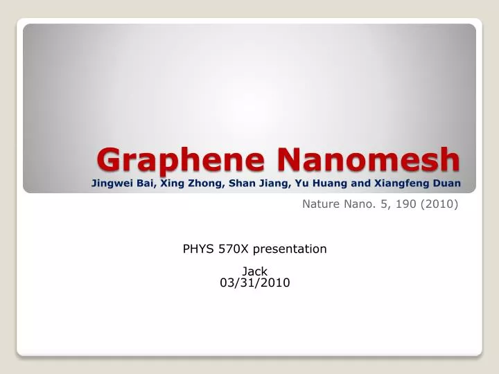
Graphene Nanomesh Jingwei Bai , Xing Zhong , Shan Jiang, Yu Huang and Xiangfeng Duan. Nature Nano . 5, 190 (2010) PHYS 570X presentation Jack 03/31/2010. Background Fabrication processes Size tunability FET measurement Summary. Outline.

E N D
GrapheneNanomeshJingweiBai, Xing Zhong, Shan Jiang, Yu Huang and XiangfengDuan Nature Nano. 5, 190 (2010) PHYS 570X presentation Jack 03/31/2010
Background • Fabrication processes • Size tunability • FET measurement • Summary Outline
Graphene is a semimetal with a zero band-gap. • Demonstrated approaches: • Graphenenanoribbon(GNR) • Graphene QDs • Drawbacks: • Low throughput • Difficulty in placement • Incompatible to semiconductor fabrication process Background Xiaolin Li, et al., Science 319, 1229 (2008)
Deposit a ~10nm SiOx (mask) Spin coat block-copolymer P(S-b-MMA) Anneal and develop the block-copolymer film Do RIE to penetrate the oxide layer Expose to oxygen plasma Remove the oxide mask by HF etch Fabrication of GNM
P-(S-b-MMA) copolymer Developed copolymer After RIE Graphene NM 100nm • Two geometrical parameters: • Periodicity • Neck size Fabrication of GNM 100nm
Different over-etch Different MW Characterization – Size tunability Tuning of periodicity and neck width by molecular weight of block copolymer and over-etch, respectively.
L ~ 1um W ~ 2um Periodicity ~39nm, neck width of ~10nm + Vg - Ion/Ioff ratio: ~14@ Vd = -0.1V On-state G = 550uS @ Vg = 10V P-channel behavior Characterization – FET Edge oxidation Physisorption of oxygen
FET with variation of neck width Const. Vd = 100mV Increase of Ion/Ioff ratio as the decreasing of neck width On-off ratio ~ 1 / width of current pathway Energy gap ~ 100 – 200meV
Graphenenanmesh showing semiconducting behavior was demonstrated using block copolymer lithography. GNM made by this lithography technique is large, continuous and process compatible. Electrical properties of GNM like on-off ratio is comparable to that of similar width of GNRs, but total drive current of GNM is much better. Summary