Download
1 / 32
330 likes | 592 Vues
Development of an Active Pixel Sensor Vertex Detector. H. Matis, F. Bieser, G. Rai, F. Retiere, S. Wurzel, H. Wieman, E. Yamamato, LBNL S. Kleinfelder, K. Singh, UCI H. Bichel, U. Washington. STAR Needs a Thin Vertex Detector to Measure Charm at RHIC. High precision - ~4 µm resolution

E N D
Development of an Active Pixel Sensor Vertex Detector H. Matis, F. Bieser, G. Rai, F. Retiere, S. Wurzel, H. Wieman, E. Yamamato, LBNL S. Kleinfelder, K. Singh, UCI H. Bichel, U. Washington
STAR Needs a Thin Vertex Detector to Measure Charm at RHIC • High precision - ~4 µm resolution • Low mass - 1 GeV/c particles - need low multiple scattering • Medium radiation environment - 50 krad/y - @ 40x RHIC luminosity 80 µm 40 µm 160 µm 320 µm 640 µm H. Matis (hsmatis@lbl.gov)
Active Pixel Sensor (APS) – Attractive Technology • Has same advantages of CCDs • Small pixels • Can thin wafers • Plus • Standard CMOS process • More radiation resistant • Low power • Put extra circuits on chip • Minus • New Technology • Lots to learn H. Matis (hsmatis@lbl.gov)
Epitaxial Sensor Medium • High-resistivity epitaxial silicon used as a sensor • Higher doped P bulk reflects and confines electrons • Slower, more lateral diffusion and recombination • 100% fill factor achieved H. Matis (hsmatis@lbl.gov)
CMOS APS with Epitaxial Sensor H. Matis (hsmatis@lbl.gov)
Three Example CMOS Pixel Circuits • Passive Pixel Sensor (PPS, left) • Active Pixel Sensor (APS, middle) • APS with sample and hold / shutter (right) H. Matis (hsmatis@lbl.gov)
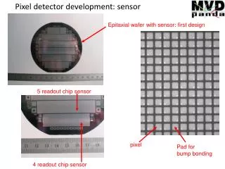
“EPI-1” Prototype Epi / APS Imager • 0.25 µm CMOS • 128 x 128 array • 4 pixel variants • 20 x 20 µm pixels • 8-10 µm Epi • Fabbed at TSMC H. Matis (hsmatis@lbl.gov)
4 Configurations • 4 variants: • Small pickup • 4x small pickups • Small pickup + direct injection • Large pickup + Direct injection H. Matis (hsmatis@lbl.gov)
APS Pixel Quadrants H. Matis (hsmatis@lbl.gov)
Sr90 Electron Source • Quadrant of 64 x 64 pixels with (left) and without (right) Sr90 source applied. H. Matis (hsmatis@lbl.gov)
1.5 GeV electron source (ALS) • Quadrant with (left) and without (right) electron source applied. H. Matis (hsmatis@lbl.gov)
Energy spectrum of 1.5 GeV electrons • Circles are measured points, dotted line shows calculated result for 8 µm epitaxial layer. H. Matis (hsmatis@lbl.gov)
Version II - 16 different configurations • Row 1 - Pixels with one to four distributed diodes. • Increase in charge collected within one pixel • Less charge diffusion to neighboring pixels • But lower gain due to increased capacitance H. Matis (hsmatis@lbl.gov)
Sample Fe55 Spectra 1638 electrons H. Matis (hsmatis@lbl.gov)
Speed Matters • Output of ADC • Currently reading a pixel with 500 kHz clock - limited by external ADC • Easily could read at 1 MHz • Need 250 ms to read out 1000 x 1000 chip with 4 channels at this speed • Working to improve speed for next generation 1 µs/division H. Matis (hsmatis@lbl.gov)
Total Collected Charge (Fe-55) H. Matis (hsmatis@lbl.gov)
Signal to Noise (Fe-55) H. Matis (hsmatis@lbl.gov)
Diode Topology vs.. Collected Charge • Normalized charge plots. • More diodes yields greater percentage of charge collected H. Matis (hsmatis@lbl.gov)
Diode Topology vs. Signal to Noise • More diodes reduces S/N except for the single pixel case (no summation of neighboring pixels) H. Matis (hsmatis@lbl.gov)
Other Configurations - Rows 2-4 Row 2 - Same as Row 1 except larger output transistor Row 3 - Centered pixel 1 small pickup 2 medium well pickup 3 large well pickup 4 large diffusion Row 4 - Sample and Hold 1 small well pickup 2 medium well pickup 3 large diffusion 4 large diffusion H. Matis (hsmatis@lbl.gov)
S/N All Sectors Row 1 Row 2 Row 3 Row 4 H. Matis (hsmatis@lbl.gov)
Charge Diffusion • Increasing number of diode collection points increases collection with lower signal • Sample and Hold collects charge in few pixels but much lower signal Row 1 - 1 diode Row 1 - 4 diode Row 4 - Sample and Hold H. Matis (hsmatis@lbl.gov)
Radiation Hardness • CCDs show radiation effects ~ krad • 3 year RHIC design luminosity - 3.5 krad or 1 x 10¹¹ 55 MeV p’s/cm • 3 year RHIC II at 40x design - 140 krad • Expose unpowered chips to 55 MeV p’s at 88” cyclotron H. Matis (hsmatis@lbl.gov)
Pre Radiation Post Radiation 1012 protons at 55 MeV Equivalent to 3 years at RHIC at 40x current luminosity H. Matis (hsmatis@lbl.gov)
30 y @ RHIC II 1.5 1011 protons, 55 MeV Equivalent to 0.5 y @ 40x current Luminosity of RHIC (RHIC II) 9 y @ RHIC II 3 y @ RHIC II 1.5 y @ RHIC II Mrad H. Matis (hsmatis@lbl.gov)
> Mrad exposure H. Matis (hsmatis@lbl.gov)
Signal Loss to Radiation • Signal does decrease with radiation dose • Noise increases • Small change in radiation region of our interest • Significant Mrad effects H. Matis (hsmatis@lbl.gov)
Thinned Silicon • CCD detector thin to epi layer (with backing) • Testing 50 µm and 100 µm wafers • 50 µm wafer can be stretched to >1 kg (limit is our stain gauge) • Build mechanical support easy to replace modules - beam accident Silicon H. Matis (hsmatis@lbl.gov)
Mechanical Configuration H. Matis (hsmatis@lbl.gov)
Summary and Conclusions • A CMOS active pixel sensor array using an epitaxial silicon sensor has been designed and tested. • Two 128 by 128 pixel arrays were fabricated • Both used a standard digital 0.25 micron CMOS technology • Both used 8-10 micron epitaxial silicon sensors • Variety of pixel topologies and circuits were tested. • Optimum performance in sparse-event environment was obtained by simplest, highest gain pixel circuits. • Tested with 1.5 GeV electrons and Fe-55 X-rays • Obtained 13 electrons RMS noise and an SNR for single Fe-55 X-rays (5.9 keV) of greater than 30. • Standard digital CMOS APS can resolve individual gamma rays and minimum-ionizing charged particles. • CMOS technology appropriate to radiation environment of RHIC. H. Matis (hsmatis@lbl.gov)
Future • Must fully understand noise sources – improve signal to noise. Reduce charge diffusion • New faster chip in 0.5 µm process ready soon. Larger epi layer • Increase speed of chip • 1000 x 1000 array with four parallel channels - 50 ns readout 12.5 ms cycle time • Mechanical Prototyping. Fixture ready in a week. • Great promise of APS technology at RHIC H. Matis (hsmatis@lbl.gov)