Download
1 / 2
20 likes | 168 Vues
MRI : Acquisition of a State-of-the-Art Aberration-Corrected Analytical Electron Microscope with Enhanced Atomic-Level Spectrometry and Low-Voltage Performance. Masashi Watanabe, Lehigh University, DMR 1040229. Intellectual Merit

E N D
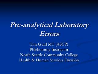
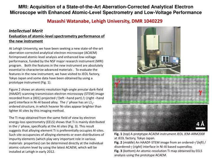
MRI: Acquisition of a State-of-the-Art Aberration-Corrected Analytical Electron Microscope with Enhanced Atomic-Level Spectrometry and Low-Voltage Performance Masashi Watanabe, Lehigh University, DMR 1040229 Intellectual Merit Evaluation of atomic-level spectrometry performance of the new instrument At Lehigh University, we have been seeking a new state-of-the-art aberration-corrected analytical electron microscope (ACAEM) forimproved atomic-level analysis and enhanced low-voltage performance, funded by the NSF major research instrument (MRI) program. Both the features in the new instrument are absolutely essential to characterize advanced materials . To evaluate the features in the new instrument, we have visited to JEOL factory, Tokyo Japan and some data have been obtained by using a prototype instrument (Fig. 1). Figure 2 shows an atomic-resolution high-angle annular dark-field (HAADF) scanning transmission electron microscopy (STEM) image recorded from a [001]-projected g’(left –hand part) /g (right –hand part) interface in Ni-Al based alloy. The g’ phase has an L12-ordered structure, in which heavier Ni-sites appear brighter than lighter Al sites by this imaging method. The Ti map obtained from the same field of view by electron energy-loss spectrometry (EELS) shows that Ti is mainly distributed in the g' phase, specifically at the Al sites (Fig. 3). This result suggests that alloying element Ti is preferentially occupies Al-sites. Such site occupancies of alloying elements or even distributions of impurity elements (which play very important role in various materials properties) can be determined directly at the individual atomic-column level by using the latest ACAEM, which will be installed at Lehigh in early 2012. g’ g 4 Å Fig. 1 (top) A protptype ACAEM instrument JEOL JEM-ARM200F at JEOL factory, Tokyo Japan. Fig. 2 (middle) An HAADF-STEM image from an ordered-g’(left) / disordered-g (right) interface in Ni-Al based superalloy. Fig. 3 (bottom) An atomic-resolution Ti map obtained by EELS analysis using the prototype ACAEM.
MRI: Acquisition of a State-of-the-Art Aberration-Corrected Analytical Electron Microscope with Enhanced Atomic-Level Spectrometry and Low-Voltage Performance Masashi Watanabe, Lehigh University, DMR 1040229 Broader Impact Development of an automated aberration-tuning method on an oriented crystalline specimen When operating an aberration-corrected STEM, it is essential to tune a corrector system, which requires anamorphous-based standard specimen. Then, the standard specimen is replaced with the sample of real interest, which is usually crystalline, and final tuning of defocus and two-fold astigmatism is performed in a manual fashion during actual observation of atomic resolution images, which is still problematic for inexperienced users. If aberrations are measurable from atomic-resolution STEM images of a real crystalline specimen directly, aberration auto-tuning can be performed instantaneously during structural observation. Therefore, the PI has developed a aberration tuning procedure named a segmented image auto-correlation function matrix (SIAM) method with Dr. Hidetaka Sawada, JEOL. This procedure can be run under widely used GatanDigitalMicrographdoftware (Fig. 4). Figure 5 compares high-resolution HAADF-STEM images of SrTiO3before (top) and after (bottom) applying the SIAM method, which were taken in the JEM-ARM200F prototype instrument. By applying the SIAM method , the atomic-resolution lattice fringes now appear clearly without any manual adjustment. This tool will be used for training new users on how to tune the corrector. Fig. 4(left) A dialog for the SIAM method implemented in GatanDigitalMicrograph. Fig. 5 (right) High resolution images of SrTiO3 before (top) and after (bottom) three iterations of SIAM process