Download
1 / 63
630 likes | 794 Vues
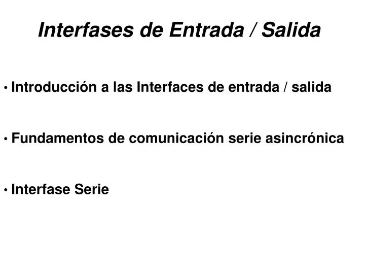
Interfases de Entrada / Salida. Introducción a las Interfaces de entrada / salida Fundamentos de comunicación serie asincrónica Interfase Serie. Introducción a las Interfaces de entrada / salida. Puerto de Salida Básico. Registro (Latch). CE. CLK. WR. OE. D0 D7. Q0 Q7.

E N D
Interfases de Entrada / Salida • Introducción a las Interfaces de entrada / salida • Fundamentos de comunicación serie asincrónica • Interfase Serie
Introducción a las Interfaces de entrada / salida
Puerto de Salida Básico Registro (Latch) CE CLK WR OE D0 D7 Q0 Q7 Bus de Datos del Sistema Salidas
Sintesis en vhdl de un puerto de salida Entity Salida is port ( HCLK : in std_logic; RESET : in std_logic; CS : in std_logic; WR : in std_logic; D : in std_logic_vector (7 downto 0); --Bus datos es siempre entrada O : out std_logic_vector (7 downto 0) --Salidas al exterior ); end Salida;
architecture B2 of Salida is begin process (HCLK, RESET) begin if RESET = '1' then O ( 7 downto 0 )<= "00000000"; else if HCLK = '1' and HCLK'event then -- Flanco de ascendente if CS = '0' then if WR = '0' then O (7 downto 0) <= D ( 7 downto 0 ); end if; end if; end if; end if; end process; end B2;
Puerto de Entrada Básico Puerta de 3 estados (Transceiver) CE OE RD O0 O7 I0 I7 Bus de Datos del Sistema Entradas
Sintesis en vhdl de un puerto de entrada entity Entrada is port ( HCLK : in std_logic; RESET : in std_logic; CS : in std_logic; RD : in std_logic; D : out std_logic_vector (7 downto 0); -- Bus Datos es siempre salida I : in std_logic_vector (7 downto 0) -- Entradas externas ); end Entrada;
architecture B2 of Entrada is Begin process (HCLK, RESET) Begin if RESET = '1' then D ( 7 downto 0 )<= "ZZZZZZZZ"; else if HCLK = '1' and HCLK'event then -- Flanco de ascendente if CS = '0' then -- Acceso al registro solo si CS es 0 if RD = '0' then D ( 7 downto 0 ) <= I (7 downto 0); else D ( 7 downto 0 ) <="ZZZZZZZZ"; -- Si RD esta en 1 el bus esta en "Z" end if; else D ( 7 downto 0 ) <="ZZZZZZZZ"; -- Si CS esta en 1 el bus esta en "Z" end if; end if; end if; end process; end B2;
Sintesis en vhdl de un registro interno entity Registro is port ( HCLK : in std_logic; RESET : in std_logic; CS : in std_logic; RD : in std_logic; WR : in std_logic; D : inout std_logic_vector (7 downto 0) -- Bus de datos es Entrada/Salida ); end Registro;
architecture B2 of Registro is Begin process (HCLK, RESET) variable REGISTRO : std_logic_vector (7 downto 0) := "00000000"; Begin if RESET = '1' then D ( 7 downto 0 )<= "ZZZZZZZZ"; else if HCLK = '1' and HCLK'event then -- Flanco de ascendente if CS = '0' then -- Acceso al registro solo si CS es 0 if RD = '0' then D ( 7 downto 0 ) <= REGISTRO (7 downto 0); else D ( 7 downto 0 ) <="ZZZZZZZZ"; -- Si RD = 1, bus en "Z" if WR = '0' then REGISTRO (7 downto 0) := D ( 7 downto 0 ); end if; end if; else D ( 7 downto 0 ) <="ZZZZZZZZ"; -- Si CS = 1, bus en "Z" end if; end if; end if; end process; end B2;
entity PWM is port ( HCLK : in std_logic; RESET : in std_logic; CS : in std_logic; RD : in std_logic; WR : in std_logic; D : inout std_logic_vector (7 downto 0); PWM : out std_logic ); end PWM;
architecture B2 of PWM is Begin process (HCLK, RESET) variable REGISTRO : std_logic_vector (7 downto 0) := "00000000"; variable CICLO : std_logic_vector (7 downto 0) := "00000000"; variable CONTADOR : std_logic_vector (7 downto 0) := "00000000"; Begin if RESET = '1' then D ( 7 downto 0 )<= "ZZZZZZZZ"; PWM <= '0'; else if HCLK = '1' and HCLK'event then -- Flanco de ascendente if CS = '0' then -- Acceso al registro solo si CS es 0 if RD = '0' then D ( 7 downto 0 ) <= REGISTRO (7 downto 0); else D ( 7 downto 0 ) <="ZZZZZZZZ"; -- Si RD es 1 el bus es "Z" if WR = '0' then REGISTRO (7 downto 0) := D ( 7 downto 0 ); end if; end if; else D ( 7 downto 0 ) <="ZZZZZZZZ"; -- Si CS es 1 el bus es "Z" end if;
CONTADOR := CONTADOR +1; if CONTADOR > CICLO then PWM <= '0'; else PWM <= '1'; end if; if CONTADOR = "00000000" then CICLO := REGISTRO; end if; end if; end process; end B2;
Puerto de Entrada + Salida Básico CE Registro (Latch) WR OE Salida Bus de Datos Entrada Puerta de 3 estados (Transceiver) OE RD
Puerto de Entrada + Salida Básico CE Registro (Latch) WR OE Salida Bus de Datos Entrada Puerta de 3 estados (Transceiver) OE RD
Puerto de Entrada / Salida Programable CE Registro (Latch) WR OE Exterior Salida Bus de Datos Entrada Puerta de 3 estados (Transceiver) OE RD
Puerto de Entrada / Salida Programable CE 1 WR OE Exterior CE WR OE Salida Bus de Datos Entrada OE RD
Puerto de Entrada / Salida Programable A0 WR OE CE Exterior WR OE Salida Bus de Datos Entrada OE RD
Puerto de Entrada / Salida Programable CE A0 WR RD OE Lógica de control de lectura y escritura (LCLE) Exterior OE Salida Bus de Datos Entrada OE
Puerto de Entrada / Salida Programable CE A0 WR RD OE Lógica de control de lectura y escritura (LCLE) Exterior OE Salida Bus de Datos Entrada OE
Puerto de Entrada / Salida Programable CE A0 WR RD OE LCLE Puerta bidireccional de 3 estados (Transceiver) OE Salida OE Dd Entrada Bus de Datos del sistema OE
Puerto de Entrada / Salida Programable con Reset RESET CE A0 WR RD OE LCLE Puerta bidireccional de 3 estados (Transceiver) OE Salida OE Dd Entrada Bus de Datos del sistema OE
Puerto de Entrada / Salida Programable con Reset RESET CE A0 WR RD OE LCLE Puerta bidireccional de 3 estados (Transceiver) OE Salida OE Dd Entrada Bus de Datos del sistema OE
entity IOP is port ( HCLK : in std_logic; RESET : in std_logic; CS : in std_logic; AD0 : in std_logic WR : in std_logic; RD : in std_logic; D : inout std_logic_vector (7 downto 0); -- El bus de datos es Entrada/Salida ES : inout std_logic_vector (7 downto 0) -- Entradas/Salidas al exterior ); end IOP;
architecture B2 of IOP is Begin process (HCLK, RESET) variable DDR : std_logic_vector ( 7 downto 0) :="00000000"; --entrada variable DAT : std_logic_vector ( 7 downto 0) :="00000000"; Begin if RESET = '1' then ES ( 7 downto 0 )<= "ZZZZZZZZ"; DDR ( 7 downto 0 ) := "00000000"; DAT ( 7 downto 0 ) := "00000000"; D ( 7 downto 0 )<= "ZZZZZZZZ"; else if HCLK = '1' and HCLK'event then -- Flanco de ascendente if CS = '0' then if WR = '0' then if AD0 = '0' then DAT( 7 downto 0 ) := D( 7 downto 0 ); n1: for i in 0 to 7 loop if DDR(i) = '1' then ES (i) <= D (i); else ES (i) <= 'Z'; end if; end loop n1;
else DDR( 7 downto 0 ) := D( 7 downto 0 ); n2: for i in 0 to 7 loop if D(i) = '1' then ES (i) <= DAT (i); else ES (i) <= 'Z'; end if; end loop n2; end if; else if RD = '0' then if AD0 = '0' then n3: for i in 0 to 7 loop if DDR(i) = '1' then D (i) <= DAT (i); else D (i) <= ES(i); end if; end loop n3; else D(7 downto 0) <= DDR(7 downto 0); end if; else D( 7 downto 0 ) <= "ZZZZZZZZ"; end if; end if;
else D( 7 downto 0 ) <= "ZZZZZZZZ"; end if; end if; end if; end process; end B2;
Puerto de E / S con Pedido de Atención y Banderas Habilitación INTR Bandera Puertas de 3 estados (Transceiver) 1 OE D Q R Bus de Datos OE Entrada
8. 8. 8. 8. Aplicación Q7 CE1 Excitación (Ánodos) WL CLK D7 … D0 OE Q0 CE1 WH CLK K3 K2 K1 K0 D15 … D8 Q3 Q0 OE Habilitaciones (Cátodos)
a f b g e c p d
ÁNODOS CÁTODO COMÚN ÁNODOS
Vcc a b c d e f g p CÁTODO COMÚN ÁNODOS
ÁNODOS 5. 8. 8. 8. KHH KMH KML KLL ULN2003 1 0 0 0
ÁNODOS 8. 8. 3. 8. KMH KML KLL ULN2003 0 1 0 0
ÁNODOS 8. 9. 8. 8. KMH KML KLL ULN2003 0 0 1 0
ÁNODOS 8. 8. 8. 6. KMH KML KLL ULN2003 0 0 0 1
;Subrutina DISP ;Variables utilizadas: ;STATUS : Próximo dígito de Buffer que es necesario refrescar ;BUFFER : Tabla de 8 bytes que contiene los datos para el display y los códigos de habilitación correspondientes STATUS dw 0 BUFFER db 1, 1 ;LSD , 00000001 db 3, 2 ; , 00000010 db 5, 4 ; , 00000100 db 7, 8 ;MSD; 00001000 ;PORT_A : Etiqueta que especifica la dirección del puerto del display PORT_A equ XXXX
;SUB. DE REFRESCO------------ DISP PROC NEAR XOR AX,AX MOV DX, PORT_A OUT DX,AX ;APAGA DISPLAY MOV BX, STATUS ;BUSCA DATOS EN BUFFER MOV SI, OFFSET BUFFER MOV AX,(BX+SI) OUT DX,AX ;ENCIENDE DIGITO ADD BX, 2 ;APUNTA AL PROXIMO DIGITO EN MEMORIA AND BX, 7 MOV STATUS,BX RET
;SUB. DE REFRESCO------------ DISP PROC NEAR XOR AX,AX MOV DX, PORT_A OUT DX,AX ;APAGA DISPLAY MOV BX, STATUS ;BUSCA DATOS EN BUFFER MOV SI, OFFSET BUFFER MOV AX,(BX+SI) OUT DX,AX ;ENCIENDE DIGITO ADD BX, 2 ;APUNTA AL PROXIMO DIGITO EN MEMORIA AND BX, 7 MOV STATUS,BX RET
;SUB. DE REFRESCO------------ DISP PROC NEAR XOR AX,AX MOV DX, PORT_A OUT DX,AX ;APAGA DISPLAY MOV BX, STATUS ;BUSCA DATOS EN BUFFER MOV SI, OFFSET BUFFER MOV AX,(BX+SI) OUT DX,AX ;ENCIENDE DIGITO ADD BX, 2 ;APUNTA AL PROXIMO DIGITO EN MEMORIA AND BX, 7 MOV STATUS,BX RET
;SUB. DE REFRESCO------------ DISP PROC NEAR XOR AX,AX MOV DX, PORT_A OUT DX,AX ;APAGA DISPLAY MOV BX, STATUS ;BUSCA DATOS EN TRABLA MOV SI, OFFSET BUFFER MOV AX,(BX+SI) OUT DX,AX ;ENCIENDE DIGITO ADD BX, 2 ;APUNTA AL PROXIMO DIGITO EN MEMORIA AND BX, 7 MOV STATUS,BX RET
;SUB. DE REFRESCO------------ DISP PROC NEAR XOR AX,AX MOV DX, PORT_A OUT DX,AX ;APAGA DISPLAY MOV BX, STATUS ;BUSCA DATOS EN TRABLA MOV SI, OFFSET BUFFER MOV AX,(BX+SI) OUT DX,AX ;ENCIENDE DIGITO ADD BX, 2 ;APUNTA AL PROXIMO DIGITO EN MEMORIA AND BX, 7 MOV STATUS,BX RET