Download
1 / 27
300 likes | 434 Vues
Logic Design / Processor and Control Units. Tony Diep. Topics to be discuss…. Functional properties of digital integrated circuits Instruction sets Number presentation Register and ALU organization Data paths. Logic Gates.

E N D
Topics to be discuss… • Functional properties of digital integrated circuits • Instruction sets • Number presentation • Register and ALU organization • Data paths
Logic Gates • Binary information is represented in digital computer called signals. • Electrical signal as voltages are chosen to represent 2 recognizable states 0.5 volt = 0, 1.5 volt = 1
Logic Gates • Gates are logic circuits that manipulate binary information. • Gates are blocks of hardware that produce signals of binary 1 or 0 when input logic requirement are satisfied.
Logic Gates • NAND gate • NOR gate • Exclusive OR
Combinational & Sequential Circuits • A CC can be described by a truth table is having the binary relationship when the n input variables and the m output variable. • A SC employ signals that affect storage elements (flip-flop) only at discrete instants of time. Synchronization is achieved by time device called clock pulse generator that produces periodic train of clock pulses.
Flip - Flop • Flip-flop is part of the electronic component responsible for the storage of data in memory. • SR, JK, D flip-flops • Difference among various flip-flops is in the number of inputs they possess and the manner in which inputs affect the binary state.
Simple SR Flip-Flop • A "set/reset" flip-flop in which activating the "S" input will switch it to one stable state and activating the "R" input will switch it to the other state.
JK Flip-Flop • An edge triggeredSR flip-flop with extra logic such that only one of the R and S inputs is enabled at any time. This prevents a race condition which can occur when both inputs of an RS flip-flop are active at the same time. In a JK flip-flop the R and S inputs are renamed J and K. The set input (J) is only enabled when the flip-flop is reset and K when it is set.
D Flip-Flop • A digital logic device that stores the status of its "D" input whenever its clock input makes a certain transition (low to high or high to low). The output, "Q", shows the currently stored value.
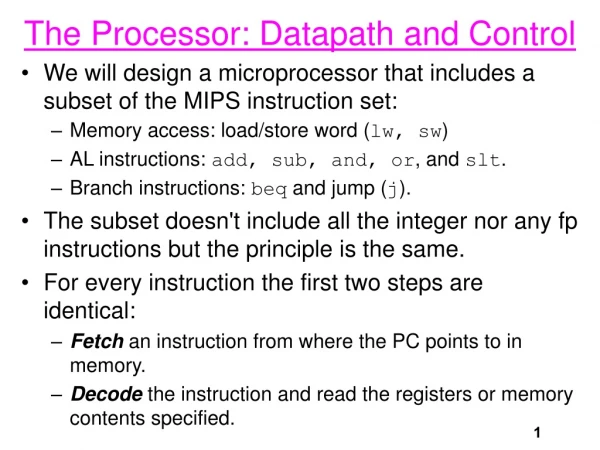
Instruction Set • Vocabulary of machine language. • Popular MIPS instruction set used Sony, NEC, Silicon Graphic.
MIPS Instruction • Million Instructions Per Second (MIPS) • Operates on two source operands and places the result in one destination operand. • Translation from C to MIPS assembly language instructions is performed by compiler.
Simples MIPS Instructions • add a, b, c -- meaning a = b + c • sub a, b, c -- meaning a = b - c • C statement -- f=(g+h) – (i+j) • add t0, g, h #temp variable t0 contains g+h add t1, i, j #temp variable t1 contains i+j sub f, t0, t1 #f gets t0 – t1, which is (g+h) - (i+j)
Number Representation • Base 2 representation • Example: 1011 base 2 in a MIPS word (32 bits) is
Unsigned and Sign • Two’s complement -- meaning leading 0s mean positive, and leading 1s mean negative. • Sign bit determine a number is positive or negative (with 0 considered positive)
Addition and Subtraction • Addition in binary starts from right to left, with carries passed to the next digit to the left. • Subtracting can be done directly such as 7 – 6, or via addition using the two’s complement representation of –6.
ALU • Arithmetic Logic Unit • A device that performs the arithmetic operations like addition and subtraction or logical operation like AND and OR. • ALU can be constructed w/ 4 hardware building blocks (AND, OR, Inverter, and Multiplexor).
1-Bit ALU • 1-bit ALU for AND and OR
1-Bit Adder 1-bit adder has 3 inputs and 2 outputs.
1-Bit ALU w/ Addition 1-bit ALU that performs AND, OR, and addition.
32-bit ALU A 32-bit ALU constructed from 32 1-bit ALUs
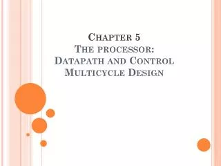
Building Data Path • For every instruction, the first 2 steps are identical: • Send the Program Counter (PC) to the memory that contains the code and fetch the instruction from that memory • Read one or two registers, using fields of the instruction to select the registers to read.
Building Data Path An abstract view of the implementation of the MIPS subset. PC supplies instruction address to the instruction memory Register operands can be operated on to compute a memory address (for load or store) Register operands used by an instruction are specified by fields of that instructions If the instruction is an arithmetic-logical instruction, the result from the ALU must be written to a register
Reference • CS 444 Lecture Notes • Computer Organization & Design by David Patterson and John L Hennessy • http://www.brunel.ac.uk/~castjjg/hndcfund/material/logic/part5.htm