Download
1 / 54
1.87k likes | 5.4k Vues
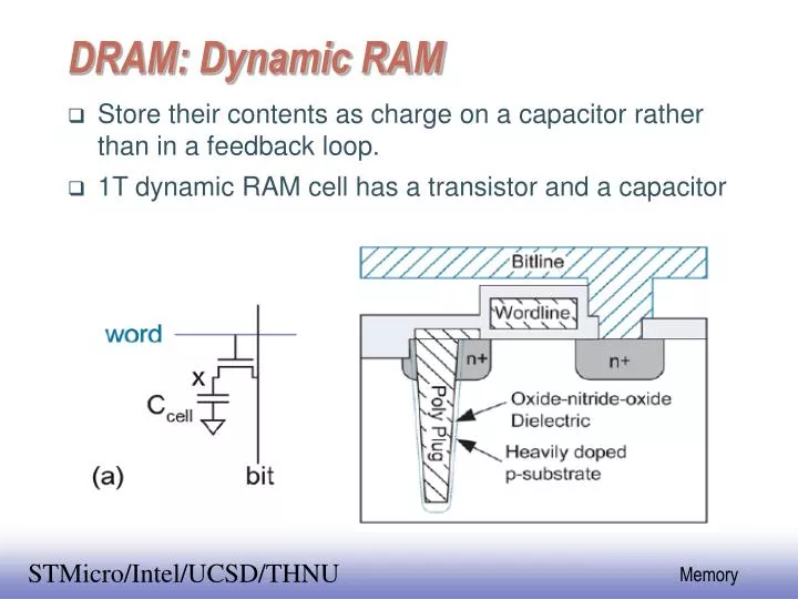
DRAM: Dynamic RAM. Store their contents as charge on a capacitor rather than in a feedback loop. 1T dynamic RAM cell has a transistor and a capacitor. DRAM Read. 1. bitline precharged to V DD /2 2. wordline rises, cap. shares it charge with bitline, causing a voltage V

E N D
DRAM: Dynamic RAM • Store their contents as charge on a capacitor rather than in a feedback loop. • 1T dynamic RAM cell has a transistor and a capacitor
DRAM Read 1. bitline precharged to VDD/2 2. wordline rises, cap. shares it charge with bitline, causing a voltage V 3. read disturbs the cell content at x, so the cell must be rewritten after each read
DRAM write On a write, the bitline is driven high or low and the voltage is forced to the capacitor
DRAM • Bitline cap is an order of magnitude larger than the cell, causing very small voltage swing. • A sense amplifier is used. • Three different bitline architectures, open, folded, and twisted, offer different compromises between noise and area.
DRAM in a nutshell • Based on capacitive (non-regenerative) storage • Highest density (Gb/cm2) • Large external memory (Gb) or embedded DRAM for image, graphics, multimedia… • Needs periodic refresh -> overhead, slower
bit (data) lines r o w d e c o d e r Each intersection represents a 1-T DRAM Cell RAM Cell Array word (row) select Column Selector & I/O Circuits row address Column Address data Classical DRAM Organization (square)
Logic Diagram of a Typical DRAM RAS_L CAS_L WE_L OE_L A 256K x 8 DRAM • Control Signals (RAS_L, CAS_L, WE_L, OE_L) are all active low • Din and Dout are combined (D): • WE_L is asserted (Low), OE_L is disasserted (High) • D serves as the data input pin • WE_L is disasserted (High), OE_L is asserted (Low) • D is the data output pin • Row and column addresses share the same pins (A) • RAS_L goes low: Pins A are latched in as row address • CAS_L goes low: Pins A are latched in as column address • RAS/CAS edge-sensitive D 9 8
Word Line C ... Bit Line Sense Amp DRAM Operations • Write • Charge bitline HIGH or LOW and set wordline HIGH • Read • Bit line is precharged to a voltage halfway between HIGH and LOW, and then the word line is set HIGH. • Depending on the charge in the cap, the precharged bitline is pulled slightly higheror lower. • Sense Amp Detects change • Explains why Cap can’t shrink • Need to sufficiently drive bitline • Increase density => increase parasiticcapacitance
RAS_L CAS_L WE_L OE_L A 256K x 8 DRAM D 9 8 RAS_L DRAM Read Timing • Every DRAM access begins at: • The assertion of the RAS_L • 2 ways to read: early or late v. CAS DRAM Read Cycle Time CAS_L A Row Address Col Address Junk Row Address Col Address Junk WE_L OE_L D High Z Junk Data Out High Z Data Out Read Access Time Output Enable Delay Early Read Cycle: OE_L asserted before CAS_L Late Read Cycle: OE_L asserted after CAS_L
RAS_L DRAM Write Timing RAS_L CAS_L WE_L OE_L A 256K x 8 DRAM • Every DRAM access begins at: • The assertion of the RAS_L • 2 ways to write: early or late v. CAS D 9 8 DRAM WR Cycle Time CAS_L A Row Address Col Address Junk Row Address Col Address Junk OE_L WE_L D Junk Data In Junk Data In Junk WR Access Time WR Access Time Early Wr Cycle: WE_L asserted before CAS_L Late Wr Cycle: WE_L asserted after CAS_L
DRAM Performance • A 60 ns (tRAC) DRAM can • perform a row access only every 110 ns (tRC) • perform column access (tCAC) in 15 ns, but time between column accesses is at least 35 ns (tPC). • In practice, external address delays and turning around buses make it 40 to 50 ns • These times do not include the time to drive the addresses off the microprocessor nor the memory controller overhead. • Drive parallel DRAMs, external memory controller, bus to turn around, SIMM module, pins… • 180 ns to 250 ns latency from processor to memory is good for a “60 ns” (tRAC) DRAM
1-Transistor Memory Cell (DRAM) row select • Write: • 1. Drive bit line • 2.. Select row • Read: • 1. Precharge bit line • 2.. Select row • 3. Cell and bit line share charges • Very small voltage changes on the bit line • 4. Sense (fancy sense amp) • Can detect changes of ~1 million electrons • 5. Write: restore the value • Refresh • 1. Just do a dummy read to every cell. bit
DRAM technological requirements • Unlike SRAM : large Cb must be charged by small sense FF. This is slow. • Make Cb small: backbias junction cap., limit blocksize, • Backbias generator required. Triple well. • Prevent threshold loss in wl pass: VG > Vccs+VTn • Requires another voltage generator on chip • Requires VTnwl> Vtnlogic and thus thicker oxide than logic • Better dynamic data retention as there is less subthreshold loss. • DRAM Process unlike Logic process! • Must create “large” Cs (10..30fF) in smallest possible area • (-> 2 poly-> trench cap -> stacked cap)
Refreshing Overhead • Leakage : • junction leakage exponential with temp! • 2…5 msec @ 800 C • Decreases noise margin, destroys info • All columns in a selected row are refreshed when read • Count through all row addresses once per 3 msec. (no write possible then) • Overhead @ 10nsec read time for 8192*8192=64Mb: • 8192*1e-8/3e-3= 2.7% • Requires additional refresh counter and I/O control
DRAM Memory Systems n address DRAM Controller DRAM 2^n x 1 chip n/2 Memory Timing Controller w Bus Drivers Tc = Tcycle + Tcontroller + Tdriver
DRAM Performance Cycle Time Access Time Time • DRAM (Read/Write) Cycle Time >> DRAM (Read/Write) Access Time • 2:1; why? • DRAM (Read/Write) Cycle Time : • How frequent can you initiate an access? • DRAM (Read/Write) Access Time: • How quickly will you get what you want once you initiate an access? • DRAM Bandwidth Limitation: • Limited by Cycle Time
N cols Fast Page Mode Operation Column Address • Fast Page Mode DRAM • N x M “SRAM” to save a row • After a row is read into the register • Only CAS is needed to access other M-bit blocks on that row • RAS_L remains asserted while CAS_L is toggled DRAM Row Address N rows N x M “SRAM” M bits M-bit Output 1st M-bit Access 2nd M-bit 3rd M-bit 4th M-bit RAS_L CAS_L A Row Address Col Address Col Address Col Address Col Address
Page Mode DRAM Bandwidth Example • Page Mode DRAM Example: • 16 bits x 1M DRAM chips (4 nos) in 64-bit module (8 MB module) • 60 ns RAS+CAS access time; 25 ns CAS access time • Latency to first access=60 ns Latency to subsequent accesses=25 ns • 110 ns read/write cycle time; 40 ns page mode access time ; 256 words (64 bits each) per page • Bandwidth takes into account 110 ns first cycle, 40 ns for CAS cycles • Bandwidth for one word = 8 bytes / 110 ns = 69.35 MB/sec • Bandwidth for two words = 16 bytes / (110+40 ns) = 101.73 MB/sec • Peak bandwidth = 8 bytes / 40 ns = 190.73 MB/sec • Maximum sustained bandwidth = (256 words * 8 bytes) / ( 110ns + 256*40ns) = 188.71 MB/sec
4 Transistor Dynamic Memory • Remove the PMOS/resistors from the SRAM memory cell Value stored on the drain of M1 and M2 • But it is held there only by the capacitance on those nodes • Leakage and soft-errors may destroy value
First 1T DRAM (4K Density) • Texas Instruments TMS4030 introduced 1973 • NMOS, 1M1P, TTL I/O • 1T Cell, Open Bit Line, Differential Sense Amp • Vdd=12v, Vcc=5v, Vbb=-3/-5v (Vss=0v)
16k DRAM (Double Poly Cell) • MostekMK4116, introduced 1977 • Address multiplex • Page mode • NMOS, 2P1M • Vdd=12v, Vcc=5v, Vbb=-5v (Vss=0v) • Vdd-Vt precharge, dynamic sensing
64K DRAM • Internal Vbbgenerator • Boosted Wordline and Active Restore • eliminate Vtloss for ‘1’ • x4 pinout
256K DRAM • Folded bitline architecture • Common mode noise to coupling to B/Ls • Easy Y-access • NMOS 2P1M • poly 1 plate • poly 2 (polycide) -gate, W/L • metal -B/L • redundancy
1M DRAM • Triple poly Planar cell, 3P1M • poly1 -gate, W/L • poly2 –plate • poly3 (polycide) -B/L • metal -W/L strap • Vdd/2 bitline reference, Vdd/2 cell plate
On-chip Voltage Generators • Power supplies • for logic and memory • precharge voltage • e.g VDD/2 for DRAM Bitline . • backgate bias • reduce leakage • WL select overdrive (DRAM)
Vin ~ +Vin dV Vin +Vin dV Vo Charge Pump Operating Principle Charge Phase +Vin Discharge Phase Vin = dV – Vin + dV +Vo Vo = 2*Vin + 2*dV ~ 2*Vin
d dV Vhi VGG=Vhi Vhi Vcf(0) ~ Vhi + VGG ~ Vhi + Vhi CL Cf Vcf ~ Vhi Voltage Booster for WL Cf CL
Backgate bias generation Use charge pump Backgate bias: Increases Vt -> reduces leakage • reduces Cj of nMOST when applied to p-well (triple well process!), smaller Cj -> smaller Cb → larger readout ΔV
Vdd / 2 Generation 2v 1v 1.5v 0.5v ~1v 1v 0.5v 0.5v 1v Vtn = |Vtp|~0.5v uN = 2 uP
4M DRAM • 3D stacked or trench cell • CMOS 4P1M • x16 introduced • Self Refresh • Build cell in vertical dimension -shrink area while maintaining 30fF cell capacitance
Samsung 64Mbit DRAM Cross Section Stacked-Capacitor Cells Poly plate COB=Capacitor over bit Hitachi 64Mbit DRAM Cross Section
BEST cell Dimensions Deep Trench etch with very high aspect ratio
256K DRAM • Folded bitline architecture • Common mode noise to coupling to B/Ls • Easy Y-access • NMOS 2P1M • poly 1 plate • poly 2 (polycide) -gate, W/L • metal -B/L • redundancy
WL direction (row) 64K cells (256x256) 1M cells = 64Kx16 Local WL Decode SA+col mux BL direction (col) Global WL decode + drivers Column predecode
DRAM Array Example (cont’d) 2048 256x256 64 256 512K Array Nmat=16 ( 256 WL x 2048 SA) Interleaved S/A & Hierarchical Row Decoder/Driver (shared bit lines are not shown)