Download
1 / 24
240 likes | 440 Vues
This presentation will probably involve audience discussion, which will create action items. Use PowerPoint to keep track of these action items during your presentation In Slide Show, click on the right mouse button Select “Meeting Minder” Select the “Action Items” tab

E N D
This presentation will probably involve audience discussion, which will create action items. Use PowerPoint to keep track of these action items during your presentation • In Slide Show, click on the right mouse button • Select “Meeting Minder” • Select the “Action Items” tab • Type in action items as they come up • Click OK to dismiss this box • This will automatically create an Action Item slide at the end of your presentation with your points entered. Surface Electronic Characterization with SPM Sidney Cohen Franco-Israel Conference on Nanocharacterization
Preview • Introduction to modes of SPM electronic characterization - • current/voltage spectroscopy (I/V), scanning spreading resistance microscopy (SSRM), scanning capacitance microscopy (SCM), scanning Kelvin microscopy (SKPM). • Examples: • Study of electronic states in Quantum dots • Study of electron transport in thin organic films • Investigation of transport at grain boundaries Franco-Israel Conference on Nanocharacterization
Why use these techniques? • Combination of high resolution imaging with electronic characterization • Possible to identify, characterize, modify, and characterize again with same probe. • BUT !!…Need to consider interaction of probe with sample. Franco-Israel Conference on Nanocharacterization
Current-Voltage Spectroscopy I • dI/dV gives directly local density of electronic states. • Possible influence of measurement (band bending, charging) • Difference between I/V in STM/SFM Franco-Israel Conference on Nanocharacterization
I/V spectroscopy Fermi Level DOS eV =Bias voltage = energy Franco-Israel Conference on Nanocharacterization
Contact Resistance (a=contact radius, =electron mean free path Contact resistance) 1. Spreading resistance, 2. Sharvin (Ballistic) transport, Note: Franco-Israel Conference on Nanocharacterization
For typical experimental values, metals: But measure (Contaminants, oxidation, etc) Franco-Israel Conference on Nanocharacterization
Modes based on capacitative force • Scanning Capacitance Microscopy • Scanning Kelvin Probe Microscopy • Forces are long-range. Finite size of tip causes broadening of features. Franco-Israel Conference on Nanocharacterization
Scanned Probe Measurements of CdSe Quantum dot Structures* • Want to correlate size of dot with electronic properties • Due to confinement, gap varies inversely with size: • bulk Eg • *Alperson, Cohen,Rubinstein, Hodes, Phys. Rev. B 52 Localization energy Franco-Israel Conference on Nanocharacterization
I/V spectroscopy on CdSe Q. Dot Gap 1 0.15 eV Gap 2, 0.2 eV Eg=2.1 V Franco-Israel Conference on Nanocharacterization
Double capacitor configuration 4 nm gaps in parallel gives C = 6e-19. This translates to charging energy of 0.15 eV Supports premise that each peak corresponds to addition of electron to quantum dot “Coulomb Charging” Franco-Israel Conference on Nanocharacterization
Size Distribution vs. Msd. Energy Gap TEM This Exp.,with Calculated Gap Franco-Israel Conference on Nanocharacterization
Work Function Variations on thin film surfaces* • May be expected due to microscopic domain structure • SKPM can be used to detect domains with different work function down to 50 nm size. • Evidence supports domain existence: • Macroscopic Kelvin Msmts. Cannot give the spatial resolution • * Cohen, Efimov, Dimitrov, Trakhtenberg, Naaman, • submitted Franco-Israel Conference on Nanocharacterization
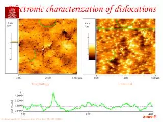
Microscopic Domain Structure in Mixed Film Franco-Israel Conference on Nanocharacterization
Results show NO variation of signal across surface Topography Raw SKPM Contrast < 5 mV Corrected SKPM Franco-Israel Conference on Nanocharacterization
Contact Potential Differences on Different Surfaces Monolayer types CN MIX3 MIX2 MIX 1 RL858 OM Mstm. 1 -600 -260 210 20 410 450 (mV) Msmt. 2 -640 -300 190 -40 360 500 (mV) Monolayer = Lewis Acid Lewis Base CPD is of tip relative to surface. More negative CPD therefore corresponds to higher work function because monolayers have extracted electrons from the gold substrate. Franco-Israel Conference on Nanocharacterization
Electron Transport at grain boundaries in semiconductors* For polycrystalline semiconductors, the electron transport properties across grain boundaries play a significant role in solar cell function, and particularly in their degradation. Crystallites can be a fraction of a micron in size, making it difficult to determine these transport properties by conventional means. Scanning Spreading Resistance, I/V spectroscopy, and SKPM can give this information *I. Visoly-Fisher, D. Cahen, S. Cohen (samples from C. Farakadis Franco-Israel Conference on Nanocharacterization
Electronic properties of Grain Boundaries can be measured by: 1. Comparing I/V curves across the grain boundary 2. Monitoring change in surface potential across boundary with SKPM Franco-Israel Conference on Nanocharacterization
Spatially-resolved I/V spectroscopy on CdTe film Using conducting SFM 2 1 3 Forward-biased currents are highest near grain boundary. May be due to lower gap energy or higher carrier concentration Franco-Israel Conference on Nanocharacterization
SKPM - Contrast in CPD image CdTe with Molecular Layer contrast = 15 meV Uncoated CdTe contrast = 30 meV Franco-Israel Conference on Nanocharacterization
Conclusions • SPM can give useful information on the nanoscale surface electronic properties • Correlation can be made between topography and electronic characteristic • Knowledge of the effect of measurement on the system is required to interpret results • Many possibilities untouched here (photo-effects, direct capacitance msmt., STM UHV work) Franco-Israel Conference on Nanocharacterization
Acknowledgements Quantum Dot Work - I. Rubinstein, G. Hodes, B. Alperson Organic Films - R. Naaman, D. Dimitrov Photovoltaics - D. Cahen, I. Visoli-Fisher All work performed at: Franco-Israel Conference on Nanocharacterization