Download
1 / 70
710 likes | 952 Vues
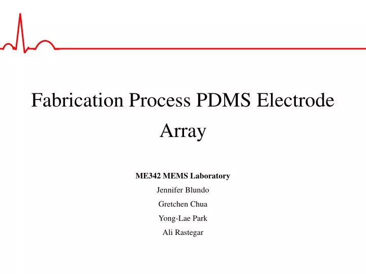
Fabrication Process PDMS Electrode Array. ME342 MEMS Laboratory Jennifer Blundo Gretchen Chua Yong-Lae Park Ali Rastegar. Project Goal.

E N D
Fabrication Process PDMS Electrode Array ME342 MEMS Laboratory Jennifer Blundo Gretchen Chua Yong-Lae Park Ali Rastegar
Project Goal • Design a bioMEMs substrate to apply and measure electromechanical forces in the differentiation of human embryonic stem cell-derived (hESC)-cardiac myocytes (CM) hESC-CMs organized in embryoid body Contractility Electrophysiology Mechanical force Undifferentiated hESCs-Fluc-eGFP (DAPI nuclear stain) bioMEMS device
Current Microscale Devices Thin-film gold strain gauges (200nm) encapsulated in PDMS (50μm). Wen et al, 2005. Thin-film stretchable (0—15%) gold electrodes (25nm) on PDMS. Lacour et al, 2005. 64 Electrode array for extracellular recording, Multi Channel Systems Pressure actuated PDMS membrane (120μm) with S-shaped SiO2 traces. Lee et al, 2004.
BioMEMS: Device Design B. Strained state A. Unstrained state Glass/Quartz: Optically transparent baseplate PDMS: A biocompatible elastomeric polymer PPS: A biocompatible elastomeric polymer Ti: Adhesion layer for electrodes Gold: Biocompatible thin film electrodes SU-8: Transparent polymer
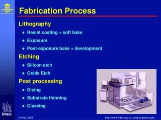
Fabrication: Baseplate Step 1:Clean Pyrex 7740 4” glass wafer (300μm thick), dehydrate 5min @ 200°C Equipment: Acetone/Methanol/IPA/DI rinse Location: MERL Glass
Fabrication: SU-8 Processing Step 2: Spin 1st layer SU-8-100(100μm thick), prebake 10min @ 65°C, softbake 30min @ 95°C, expose, postbake 1min @ 65°C, 10 min @ 95°C Equipment: Spin coater, hot plate, UV Location: MERL Channels to apply vacuum pressure to PDMS membrane Glass Glass Exposed SU-8 Unexposed SU-8
Fabrication: SU-8 Processing Step 3: Spin 2nd layer SU-8(100μm thick), prebake, expose, postbake Equipment: Spin coater, hot plate, UV Location: MERL Loading post to support PDMS membrane Glass Exposed SU-8 Unexposed SU-8
Fabrication: SU-8 Processing Step 4: Spin 3rd layer SU-8(100μm thick), prebake, expose, postbake Equipment: Spin coater, hot plate, UV Location: MERL Glass Exposed SU-8 Unexposed SU-8
Fabrication: SU-8 Processing Step 5: Spin 4th layer SU-8(80μm thick), prebake, expose, postbake Equipment: Spin coater, hot plate, UV Location: MERL Glass Exposed SU-8 Unexposed SU-8
Fabrication: SU-8 Processing Step 6: Develop SU-8, IPA/DI rinse Equipment:Location: MERL Glass Exposed SU-8
Fabrication: SU-8 Processing Step 7:Pipette tetrafluoropolymer (PS200 or T2494) to prevent PDMS membrane stiction Equipment:Location: MERL Glass Exposed SU-8 Tetrafluoropolymer
Fabrication: Baseplate Assembly Step 8: Laser cut quartz 4” wafer (300μm thick) and bond quartz over SU-8 Equipment: Laser cutter Location: MERL 20μm clearance between loading post and PDMS membrane Glass/Quartz Exposed SU-8
PDMS Electrode Array Process Option 1—Top to Bottom Photoresist
Fabrication: PDMS Membrane Step 1: Clean 4” silicon wafers Equipment:wbdiffLocation: SNF Silicon
Fabrication: PDMS Membrane Step 2: Spin sacrificial layer 5% (w/v) poly(acrylic acid) (PAA) (3000 rpm, 15 s) and bake (150C, 2 min) Equipment:Spin coater, Hot plateLocation: MERL ¼” Kapton tape at edge, removed after bake to prevent lift-off of PDMS during processing Silicon PAA
Sacrificial Layers—PDMS Micromachining • Advantages of water-soluble films • Deposited by spin-coating • The solvent removed at a low temperature (95–150C) • The resulting layer can be dissolved in water • No corrosive reagents or organic solvents • Faster release of features by lift-off • Compatible with a number of fragile materials, such as organic polymers, metal oxides and metals—materials that might be damaged during typical surface micromachining processes
BioMEMS: Fabrication Step 3:Spin thick photo resist ~ 10μm Equipment:SVGcoatLocation: SNF Silicon PAA PDMS Shadow Mask Ti Au
BioMEMS: Fabrication Step 4:Expose, develop, postbake Equipment:KarlSuss, SVGdevLocation: SNF 200μm interelectrode distance Silicon PAA PDMS Shadow Mask Ti Au 20μm diameter electrodes
BioMEMS: Fabrication Step 5: Gold deposition (2μm thick) Equipment:MetallicaLocation: SNF Silicon PAA PDMS Shadow Mask Ti Au
BioMEMS: Fabrication Step 6: Resist strip Equipment:Wbgeneral2Location: SNF Silicon PAA PDMS Shadow Mask Ti Au
BioMEMS: Fabrication Step 7: Spin photo-patternable silicone (PPS) WL5153 30sec @ 2500rpm (6μm thick), prebake 110°C Equipment:HeadwayLocation: SNF Silicon PAA PDMS Shadow Mask Ti Au
BioMEMS: Fabrication Step 8: Expose*, postbake @ 150°C**, develop, hardbake 150°C Equipment:MetallicaLocation: SNF Silicon PAA PDMS Shadow Mask Ti Au
Fabrication: Electrode Array Step 9: O2 plasma (several min)* to etch and round PPS as well as promote adhesion of metal deposition Equipment: Gasonics Silicon PAA PDMS Shadow Mask Ti Au PPS *Requires characterization
Fabrication: Electrode Array Step 10:Align beryllium copper shadow mask and temporarily bond. Equipment: EV aligner Location: SNF Silicon PAA PDMS Shadow Mask Ti Au
Fabrication: Electrode Array Step 11: Evaporate Ti adhesion layer (10nm thick), Au layer (100nm thick), Ti adhesion layer (10nm thick) Equipment: Innotec Location: SNF Maintain 200μm interelectrode distance 30μm width horseshoe tracks for electrode connections Silicon PAA PDMS Shadow Mask Ti Au 30μm diameter to allow 20μm diameter electrodes
Fabrication: Electrode Array Step 12: Remove shadow mask, O2 plasma to clean and promote adhesion Equipment:Location: SNF Silicon PAA PDMS Shadow Mask Ti Au
Fabrication: Electrode Array Step 13: Spin 20:1 Sylgard 184 poly(dimethylsiloxane) (PDMS) 90sec @ 1200 rpm (50μm thick), bake (60°C, 1 hr) Equipment:Location: MERL Silicon PAA PPS Ti Au PDMS
Fabrication: Electrode Array Step 14:Dissolve sacrificial layer PAA in water Equipment: wbgeneral Location: SNF Silicon PAA PDMS Shadow Mask Ti Au PPS
Fabrication: Electrode Array Step 15: Air dry device and transfer with handle wafer (glass) Equipment: N2 gun Location: SNF PPS PDMS Ti Au Glass
Fabrication: Assembly Step 16: O2 plasmaPDMS and quartz surfaces Equipment: Drytek PDMS PPS Ti Au Glass/Quartz SU-8
Fabrication: Assembly Step 2: Bond PDMS membrane to glass Ti Au SU-8 Glass/Quartz PDMS PPS
PDMS Electrode Array Process Option 2—Top to Bottom Skip Photoresist—Pattern PPS right on PAA, expose, deposit metal
Fabrication: Electrode Array Step 4: Spin photo-patternable silicone (PPS) WL5153 30sec @ 2500rpm (6μm thick), prebake 110°C, expose*, postbake @ 150°C**, develop, hardbake 150°C Equipment: Hot plate, Spin coater, Karl Suss*, BlueM oven**, wbgeneral Silicon PAA PDMS Shadow Mask Ti Au PPS *Proximity exposure **Need to characterize in BlueM Oven
Fabrication: Electrode Array Step 5: O2 plasma (5 min)* to etch and round PPS Equipment: Gasonics Silicon PAA PDMS Shadow Mask Ti Au PPS *Requires characterization
PDMS Electrode Array Process Option 3—Bottom to Top Pattern PDMS right on PAA, deposit metal, spin PPS, expose, O2 plasma etch down OR HCl dip if use Ti layer
Fabrication: PDMS Membrane Step 1: Clean 4” silicon wafers Equipment:wbdiffLocation: SNF Silicon
Fabrication: PDMS Membrane Step 2: Spin sacrificial layer 5% (w/v) poly(acrylic acid) (PAA) (3000 rpm, 15 s) and bake (150C, 2 min) Equipment:Spin coater, Hot plateLocation: MERL ¼” Kapton tape at edge, removed after bake to prevent lift-off of PDMS during processing Silicon PAA
Fabrication: PDMS Membrane Step 3: Spin 20:1 Sylgard 184 poly(dimethylsiloxane) (PDMS) (50μm thick), bake (60C, 1 hr), O2 plasma (1 min) Equipment:Location: MERL 2mm gap at edge of wafer to prevent lift-off of PDMS during processing Silicon PAA PDMS
Fabrication: Electrode Array Step 4:Align beryllium copper shadow mask and temporarily bond. Equipment: EV aligner Location: SNF 200μm interelectrode distance 30μm width tracks for electrode connections Silicon PAA PDMS Shadow Mask Ti Au 30μm diameter to allow 20μm diameter electrodes
Fabrication: Electrode Array Step 5: Evaporate Ti adhesion layer (10nm thick) and Au layer (100nm thick)* Equipment: Innotec Location: SNF 30μm width tracks for electrode connections Silicon PAA PDMS Shadow Mask Ti Au 30μm diameter to allow 20μm diameter electrodes *May want second layer of Ti to promote adhesion to PPS on top layer! Use an HCl dip to dissolve this
Fabrication: Electrode Array Step 6: Remove shadow mask, O2 plasma Equipment: Drytek Location: SNF Silicon PAA PDMS Shadow Mask Ti Au
Fabrication: Electrode Array Step 7: Spin photo-patternable silicone (PPS) WL5153 30sec @ 2500rpm (6μm thick), prebake 110°C, expose*, postbake @ 150°C**, develop, hardbake 150°C Equipment: Hot plate, Spin coater, Karl Suss*, BlueM oven**, wbgeneral Silicon PAA PDMS Shadow Mask Ti Au PPS *Proximity exposure **Need to characterize in BlueM Oven
Fabrication: Electrode Array Step 8: O2 plasma (5 min)* to etch and round PPS as well as promote adhesio Equipment: Gasonics PPS Silicon PAA PDMS Ti Au PPS *Requires characterization
Fabrication: Electrode Array Step 9:Dissolve sacrificial layer PAA in water Equipment: wbgeneral Location: SNF Silicon PAA PDMS Shadow Mask Ti Au PPS
Fabrication: Electrode Array Step 10: Air dry device and transfer with handle wafer (glass) Equipment: N2 gun Silicon PAA PDMS Shadow Mask Ti Au PPS
Fabrication: Assembly Step 1: O2 plasmaPDMS and quartz surfaces Equipment: Drytek Silicon PDMS PPS Ti Au Glass/Quartz SU-8
Fabrication: Assembly Step 2: Bond PDMS membrane to glass Ti Au SU-8 Glass/Quartz PDMS PPS
PDMS Electrode Array Process Option 4—Entire Device Pattern PDMS right on top of baseplate with PAA sacrifical layer, follow process option 3