Download
1 / 20
200 likes | 447 Vues
4-bit ALU . Yamei Li, Yuping Liang Hua Qu, James Hsu Advisor: Dave Parent 12/6/2005. Agenda. Introduction Project (Experimental) Details ALU Adder DFF MUX Summary Project result Lesson learned Acknowledgement. Introduction.

E N D
4-bit ALU Yamei Li, Yuping Liang Hua Qu, James Hsu Advisor: Dave Parent 12/6/2005
Agenda • Introduction • Project (Experimental) Details • ALU • Adder • DFF • MUX • Summary • Project result • Lesson learned • Acknowledgement
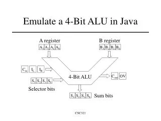
Introduction • The 4-bit ALU that our group designed can perform the following functions: • Adder, NOR, OR, and AND. • The 4-bit ALU operates at 200 MHz and use 5.8mW of Power and occupied an area of 600mm x 280mm. • The 4-bit ALU is made up of 4 identical 1-bit ALU, and 14 DFFs.
Project Description and ALU schematic • The 4-bit ALU is broken down into sub blocks consisting of: • 4 1-bit Adders • 4 4to1 MUXs • 4 AND, 4 NOR and 4 OR gate • 10 input DFFs and 4 output DFFs
Longest Path Calculations Note: All widths are in microns and capacitances in fF
MUX layout and LVS • Size of one MUX = 28mm x 70mm • Size of 4 MUX = 5% of ALU area
MUX Simulation Before Extraction • Simulation results before extraction TPHL=1.0383 ns , TPLH=1.045 ns Propagation delay < 4 LL x 0.294ns=1.177ns
MUX Post Simulation • Results from Post Extraction Simulation TPHL=0.758 ns , TPLH=0.755 ns 27% faster
Summary • After this project, we became familiar with Cadence tool and the fundamental concepts of IC design. • Our project has 338 transistors and 18 terminals. • The total area is =280mm x 600mm • The power is=3.4W/cm2 • Lessons learned • how to fix the LVS error • Learn how to work in a team • Learn how to make trade offs
Acknowledgements • Thanks to Professor D. Parent guidance and unlimited patience. • Thanks to Cadence Design Systems for the VLSI lab