Download
1 / 12
120 likes | 232 Vues
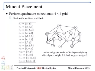
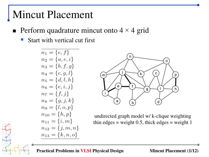
Mincut Placement. Perform quadrature mincut onto 4 × 4 grid Start with vertical cut first. undirected graph model w/ k-clique weighting thin edges = weight 0.5, thick edges = weight 1. Cut 1 and 2. First cut has min-cutsize of 3 (not unique) Both cuts 1 and 2 divide the entire chip.

E N D
Mincut Placement • Perform quadrature mincut onto 4 × 4 grid • Start with vertical cut first undirected graph model w/ k-clique weighting thin edges = weight 0.5, thick edges = weight 1 Practical Problems in VLSI Physical Design
Cut 1 and 2 • First cut has min-cutsize of 3 (not unique) • Both cuts 1 and 2 divide the entire chip Practical Problems in VLSI Physical Design
Cut 3 and 4 • Each cut minimizes cutsize • Helps reduce overall wirelength Practical Problems in VLSI Physical Design
Cut 5 and 6 • 16 partitions generated by 6 cuts • HPBB wirelength = 27 Practical Problems in VLSI Physical Design
Recursive Bisection • Start with vertical cut • Perform terminal propagation with middle third window Practical Problems in VLSI Physical Design
Cut 3: Terminal Propagation • Two terminals are propagated and are “pulling” nodes • Node k and o connect to n and j: p1 propagated (outside window) • Node g connect to j, f and b: p2 propagated (outside window) • Terminal p1 pulls k/o/g to top partition, and p2 pulls g to bottom Practical Problems in VLSI Physical Design
Cut 4: Terminal Propagation • One terminal propagated • Node n and j connect to o/k/g: p1 propagated • Node i and j connect to e/f/a: no propagation (inside window) • Terminal p1 pulls n and j to right partition Practical Problems in VLSI Physical Design
Cut 5: Terminal Propagation • Three terminals propagated • Node i propagated to p1, j to p2, and g to p3 • Terminal p1 pulls e and a to left partition • Terminal p2 and p3 pull f/b/e to right partition Practical Problems in VLSI Physical Design
Cut 6: Terminal Propagation • One terminal propagated • Node n and j are propagated to p1 • Terminal p1 pulls o and k to left partition Practical Problems in VLSI Physical Design
Cut 7: Terminal Propagation • Three terminals propagated • Node j/f/b propagated to p1, o/k to p2, and h/p to p3 • Terminal p1 and p2 pull g and l to left partition • Terminal p3 pull l and d to right partition Practical Problems in VLSI Physical Design
Cut 8 to 15 • 16 partitions generated by 15 cuts • HPBB wirelength = 23 Practical Problems in VLSI Physical Design
Comparison • Quadrature vs recursive bisection + terminal propagation • Number of cuts: 6 vs 15 • Wirelength: 27 vs 23 Practical Problems in VLSI Physical Design