Download
1 / 14

E N D
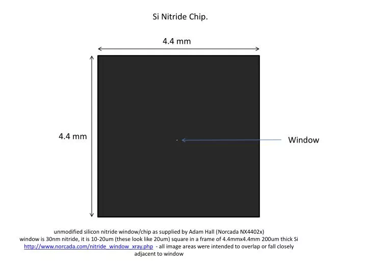
Si Nitride Chip. 4.4 mm 4.4 mm Window unmodified silicon nitride window/chip as supplied by Adam Hall (NorcadaNX4402x)window is 30nm nitride, it is 10-20um (these look like 20um) square in a frame of 4.4mmx4.4mm 200um thick Si http://www.norcada.com/nitride_window_xray.php - all image areas were intended to overlap or fall closely adjacent to window
CO samples from Marshall -origami sample 1-4 Sample 1 contains 1.7 nM origami (12ng/ul) with no extra tail extenderSample 2 contains 1.7 nM origami (12ng/ul) plus 200nm tail extension at about 1:1 ratio Sample 3 contains 1.7 nM origami (12ng/ul) plus 1200nm tail extension at about 1:1 ratio with origami Sample 4 contains ~10nM origami with 5x extra staples - this is unpurified so should have longest shelf life samples returned by Adam Hall - pores and origami (AH1-4) or just pores (AH5a and 5b) AH1 5x5, 400 nm sep, origami sample 1, measured in 1 M KCl w/ TE and MgCl2 (this is the source of the sample trace and of the one AFM image I sent) AH2 5x5, 400 nm sep, origami sample 2, measured in 50 mMKCl w/ TE and MgCl2 AH3 5x5, ~2.5 um sep, origami sample 1, measured in 1 M KCl w/ TE and MgCl2 AH4 5x5, ~1.6 um sep, origami sample 1, measured in 1 M KCl w/ TE and MgCl2 AH5a no origami 400nm sep AH5b no origami 2.8um sep
Adam Hall (AH) Samples 1, 2, and 5a. 400-nm nanopore spacing.
Adam Hall (AH) Samples 4 1600-nm nanopore spacing. AH4 - unrinsed, as recieved
Adam Hall (AH) Samples 4 1600-nm nanopore spacing. approx., location of new zoomed scan below AH4 -imaged on crystal - then Tanner rinsed surface -looked clean no more crystals - to be continued
Adam Hall (AH) Samples 4 1600-nm nanopore spacing. AH4 -imaged on crystal - then Tanner rinsed surface -looked clean no more crystals – images follow AH4 - off window
Adam Hall (AH) Samples 4 1600-nm nanopore spacing. AH4 - rinsed AH4 - off window
Adam Hall (AH) Samples 4 1600-nm nanopore spacing. AH4 -rinsed AH4 - at window
Adam Hall (AH) Samples 4 1600-nm nanopore spacing. AH4 rinsed AH4 - on window – no array visible
Adam Hall (AH) Samples 4 1600-nm nanopore spacing. AH4 -rinsed AH4 - on window - tried for dead center of window