Download
1 / 29
290 likes | 433 Vues
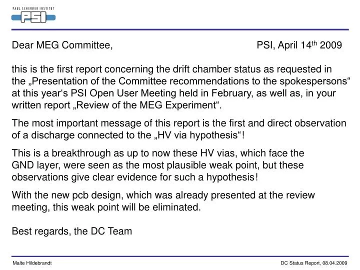
Dear MEG Committee, PSI, April 14 th 2009 this is the first report concerning the drift chamber status as requested in the „Presentation of the Committee recommendations to the spokespersons“ at this year‘s PSI Open User Meeting held in February, as well as, in your

E N D
Dear MEG Committee, PSI, April 14th 2009 this is the first report concerning the drift chamber status as requested in the „Presentation of the Committee recommendations to the spokespersons“ at this year‘s PSI Open User Meeting held in February, as well as, in your written report „Review of the MEG Experiment“. The most important message of this report is the first and direct observation of a discharge connected to the „HV via hypothesis“! This is a breakthrough as up to now these HV vias, which face the GND layer, were seen as the most plausible weak point, but these observations give clear evidence for such a hypothesis! With the new pcb design, which was already presented at the review meeting, this weak point will be eliminated. Best regards, the DC Team Malte Hildebrandt DC Status Report, 08.04.2009
dc activities in lab • helium cabin • dc01 skeleton in „aquarium“ • „via-sample“ in HV test box • next steps Malte Hildebrandt DC Status Report, 08.04.2009
DC System in Helium Cabin The next transparency summarises the activities with the dc system in the helium cabin. The important observations after ~3 more months with helium operation since the end of last years run are: • dc planes which needed to be operated with reduced HV settings at the end of run 2008 continue to deteriorate. • even planes which were still fine at the end of last years run start to deteriorate. Malte Hildebrandt DC Status Report, 08.04.2009
DC System in Helium Cabin • dc system in helium cabin • dc system inside helium environment since Jan 16th • dc modules flushed since Jan 16th: helium since Jan 30th: helium/ethane • operated with MEG dc HV system • goal: investigate HV status • compare with HV status at end of last years run • identify characteristics of weak anode channels • observations: • „weak“ planes (run 2008) get worse • „good“ planes (run 2008) start to deteriorate • characteristics of weak anode channels: similar to dc01 in „aquarium“ (Jan/Feb) → further proof for our assumptions: • HV problem related to exposure to helium • (most likely) same reason for deterioration Malte Hildebrandt DC Status Report, 08.04.2009
dc01 Skeleton in „Aquarium“ The next transparency summarises the activities with the dc01 skeleton in the „aquarium“. The dc skeleton was operated ~2 months („equivalent“ running conditions) inside the „aquarium“. The most important observation is the discharge between HV via and GND layer on the bottom side of the HV pcb! There are some more transparencies to remind you about the „via hypothesis“. Malte Hildebrandt DC Status Report, 08.04.2009
dc01 Skeleton in „Aquarium“ • dc01 skeleton: anode middle cathode anode (no hood cathode) • since Feb 19th mounted inside „aquarium“ • Feb 19th – Mar 6th: helium(30 days) Mar 6th – Mar 9th: helium / ethane (3 days) Mar 9th: HV tests („rather“ stable) Mar 9th – Mar 20th: helium (22 days) since Mar 20th: helium / ethane (until Mar 30th: 10 days) since Mar 23rd: HV tests → Mar 30th: dc01A: first direct / optical observation of discharges between HV via and GND surface on bottom side of HV pcb • trip during night at 1850 V • to match with exposure time of digital camera increase HV to 2000 V → characteristics of signals on oscilloscope same as in Jan / Feb when complete dc01 was tested in „aquarium“ but now: no hood, no G10 isolators → 65 days „run conditions“ (up to Mar 30th) ! Malte Hildebrandt DC Status Report, 08.04.2009
HV Via top layer GND +HV bottom layer 7 mm Malte Hildebrandt MEG Review Meeting, 18.02.2009
dc01A glue no glue no glue Malte Hildebrandt MEG Review Meeting, 18.02.2009
He / C2H6 He air glue glue glue G10 isolator glue G10 isolator glue carbon frame PCB Cross Section bottom layer top layer pcb pcb bottom layer +HV +HV GND Malte Hildebrandt MEG Review Meeting, 18.02.2009
dc01A anode 3 Malte Hildebrandt DC Status Report, 08.04.2009
dc01A anode 3 Malte Hildebrandt DC Status Report, 08.04.2009
dc01A anode 2 Malte Hildebrandt DC Status Report, 08.04.2009
dc01A anode 2 Malte Hildebrandt DC Status Report, 08.04.2009
dc01A anode 3 Malte Hildebrandt DC Status Report, 08.04.2009
dc01A anode 3 Malte Hildebrandt DC Status Report, 08.04.2009
HV Print 2009 The next transparency explains some of the modifications which are already implemented in the design of the new HV anode pcb in order to avoid this weak point on the bottom layer. These changes were already presented in the review meeting in February, this is just a reminder. Malte Hildebrandt DC Status Report, 08.04.2009
HV Print 2009 pads for resistors HV print 2009 • traces for HV on middle layer → no HV traces on bottom layer only GND on bottom layer → individual layers with „only HV“ or „only GND“ (3-layer → 4-layer pcb) • „blind vias“ → vias have only necessary depth to connect appropriate layers (like „blind hole“) print 2007 outer edge inner edge +HV traces vias for +HV GND print 2009 Malte Hildebrandt MEG Review Meeting, 18.02.2009
„Via Discharge“ The direct observation of discharges between HV vias and GND is the first „positive“ observation during all of these investigations. Up to now we had a long list of suspicious and possible weak points concerning the construction and operation of the drift chambers. Numerous tests during the last months have excluded step by step the „most common suspects“ from this list, with one main point remaining on the list: the bottom layer of anode HV pcb where the HV-via faces the GND-layer. The observation of these discharge is the first positive evidence during these investigations! Malte Hildebrandt DC Status Report, 08.04.2009
„Via Sample“ in HV Test Box Certainly, there are still some open questions. For example: why do the „via samples“ in the HV test box, which have no glue on the via copper ring not discharge immediately? Helium should penetrate rather fast, as there is an „open“ channel. The situation of the HV test box is summarised in the next transparency. Malte Hildebrandt DC Status Report, 08.04.2009
„Via Sample“ in HV Test Box • 2 pcb samples installed in HV test box 1st pcb: 3 vias without glue on via copper ring 4 vias with glue only on via copper ring 2nd pcb: 4 vias with glue on via copper ring and with glue in via hole • since Mar 3rd mounted inside HV test box • flushed with pure helium interruptions: Mar 9th (sealing of HV feedthroughs) Mar 14th (sealing of GND on pcb) • HV applied • T = 40-45° C(partially off from Mar 16th to 30th due to broken heating blanket) → not yet a clear result → test will continue → 50 days „run conditions“ (up to Mar 30th) Malte Hildebrandt DC Status Report, 08.04.2009
„Via Sample“ in HV Test Box • 2 pcb samples installed in HV test box 1st pcb: 3 vias without glue on via copper ring → why are there no discharges? He expected situation: pcb pcb +HV +HV GND glue G10 isolator glue Malte Hildebrandt DC Status Report, 08.04.2009
„Via Sample“ in HV Test Box There is one possible explanation for this situation: The edge of the GND layer may be somehow passivated with glue (as shown in the next transparency). This situation may be caused by the special way of applying the glue on the GND layer whereas the HV via copper ring is protected. Malte Hildebrandt DC Status Report, 08.04.2009
„Via Sample“ in HV Test Box • 2 pcb samples installed in HV test box 1st pcb: 3 vias without glue on via copper ring → why are there no discharges? He possible situation: pcb pcb +HV +HV GND glue G10 isolator glue Malte Hildebrandt DC Status Report, 08.04.2009
HV Via To answer this question we prepared another „via sample“. It was ensured that the glue was not applied on the edge of the GND layer and the via copper ring. Malte Hildebrandt DC Status Report, 08.04.2009
HV Via protection with tape before application of glue free edges of GND layer after glueing Malte Hildebrandt DC Status Report, 08.04.2009
New „Via Sample“ in HV Test Box • new pcb samples installed in HV test box 3rd pcb: 7 vias without glue on via copper ring and edge of GND layer He new situation: pcb pcb +HV +HV GND glue G10 isolator glue Malte Hildebrandt DC Status Report, 08.04.2009
New „Via Sample“ in HV Test Box → observation: after a few hours of flushing the HV test box with helium we observe the discharges between HV via and (not passivated) GND edge. top layer of pcb is covered with (red) capton tape in order to isolate / shield HV and GND on top layer rectangular cut out of the capton tape to allow helium to penetrate through the via hole into the gap between HV via and GND layer discharge in via sample mounted in HV test box → conclusion: in case of the previous „via samples“ in the HV test box, most likely the edge of the GND layer is passivated with glue and consequently no discharges will occur! Malte Hildebrandt DC Status Report, 08.04.2009
Further Tests in HV Test Box → Even the new pcb design, which will be used for chamber construction, will avoid this weak point of HV via and GND layer, we will continue with tests in the HV test box to understand better the reason for the accumulation of helium in this gap between HV via and GND layer. This will also include tests concerning the relation of breakdown voltage and gas mixture/pressure inside this gap. Malte Hildebrandt DC Status Report, 08.04.2009
Next Steps The pcb with the modified layout is ordered and is expected to arrive in the week after Easter. There is a small delay compared to the schedule presented at the review meeting. This is caused by intensive discussions (e.g. with the experts from the Pisa group) about further potential modifications of the design in order to avoid any other possible weak point. A new test is planned which represents a cross section through the wing of a dc plane and the transition of anode frame - isolators - pcb - G10 isolator (small) - G10 isolator (wide) - hood frame in order to exclude a „hidden“ discharge problem within this sandwich structure due to unexpected polarisation effects. Immediately after the delivery of the new pcb two „new“ anode wire frames will be constructed (wires are already prepared on take-over frames). Together with recycled hood cathodes and middle cathodes two new dc modules will be assembled and they will be placed inside the „aquarium“ for a long term test. In parallel we will then continue the repair work of the remaining dc modules as presented at the review meeting. Malte Hildebrandt DC Status Report, 08.04.2009