Download
1 / 19
210 likes | 376 Vues
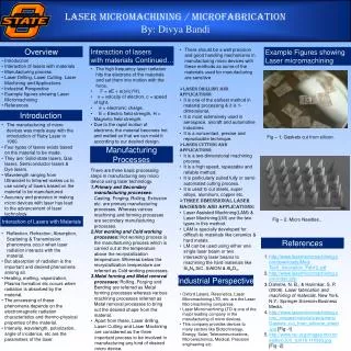
Microfabrication Technologies. Luiz Otávio Saraiva Ferreira LNLS lotavio@lnls.br. OUTLINE. Lithography Transfer of Patterns Bulk Silicon Micromachinning Surface Micromachinning LIGA technique. Litography - Evolution. France, 1822 Graphic arts. Printed circuit board- 1940-1945.

E N D
Microfabrication Technologies Luiz Otávio Saraiva Ferreira LNLS lotavio@lnls.br
OUTLINE • Lithography • Transfer of Patterns • Bulk Silicon Micromachinning • Surface Micromachinning • LIGA technique
Litography - Evolution • France, 1822 • Graphic arts. • Printed circuit board- 1940-1945. • 0.1mm wide lines. • (It may be used for microfluidics). • Integrated circuit - 1961. • 5um wide lines. • Wide evolution on electronics industry. • Microsystems require progress on 3D lithography.
Lithographic Masks • Stencil UV LIGHT 1:1 IMAGE GLASS OR QUARTZ LIGHT ABSORBER (800A Cr) PHOTORESIST SUBSTRATE • Light Field • Dark Field
Photoresist processing • Spinning • Most used substrate: Si/SiO2 • Si Oxidation • Wet or dry. • Between 900 and 1150oC. • SiO2 masks the substrate in the following processing steps. PHOTORESIST SiO2 Si SUBSTRATE
Transfer of Patterns Photoresist SiO2 Si 1 2 Radiation Unexposed Photoresist Glass Metal 4 3 5 6
Mask Aligner Karl Suss MA4
Ultra Violet or X-Ray Source 3D LithographyTechniques Mask Before Exposure Exposure After Development Thornell & Johansson, J. Micromech. Microeng. (1998) 251-262
ANISOTROPIC ISOTROPIC Bulk Silicon Micromachining A B Isotropic Selective Anisotropic Sci. Am. April 1983 pp. 39 Wet or Dry Etch
Back and Front Side Bulk Micromachining Suspensedevices Membrane Back Side Etch Cantilever Front Side Etch
Corner Compensation No compensation Beginning etch Mid etch End of etch
Surface Micromachining Etch Before etch Bridge Cantilever After etch
LIGA Technology Germany - 80’s Mold Insert Synchrotron Radiation Mold Material Mask membrane Absorber structure PLASTIC MOLDING Resist Plastic Structure (Lost Mold) Base Plate DEMOLDING IRRADIATION Ceramic Slurry Resist structure Base Plate DEVELOPMENT Plastic Structure (Lost Mold) Metal SLURRY CASTING Resist Structure Ceramic Micro-structure Base Plate ELECTROFORMING Mold Insert FIRING Metal Mold Cavity Plastic Structure MOLD FABRICATION Mold Insert Gate Plate ELECTROFORMING Mold Material Injection Hole Gate Plate Metallic Micro-structure MOLD FILLING Injection Hole Plastic Microstructure FINISHING DEMOLDING 15
Deep X-ray Lithography X-Ray Be Filter (125um) Al Filter Kapton mask Plating Base (0.2um Au) Au absorber (1.8um) 20um SU-8 100um thick SU-8 film Si substrate 5 - 15 keV spectrum after filtering 16
Resists for deep X-ray Lithography • PMMA (polymethylmetacrylate) • the most used. • High resolution. • Low sensitivity (2.5 kJ/cm3 minimum dose). • Long exposure times. • Up to 100µm thick 1-3 keV energy. • From 100µm to 500µm thick 3 - 7 keV energy. • SU-8 (epoxy based) • a promising material • Good resolution. • High sensitivity. • Short exposure times. • Difficult processing. 17
Kapton Mask 20µm thick UV-LIGA process. Deep UV lithography on SU-8. Au platting. 2µm Au 20µm SU-8 Plating Base 25µm thick Kapton Membrane Frame 18
Deep UV lithography Deep X-ray lithography • UV • Cheap • Non-vertical sidewalls - border diffraction effect. • RX • Expensive • Vertical sidewalls - negligible border diffraction. 19