Download
1 / 16
1.13k likes | 2.19k Vues
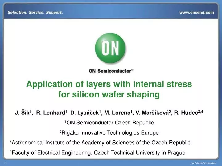
Application of layers with internal stress for silicon wafer shaping J. Šik 1 , R. Lenhard 1 , D. Lysáček 1 , M . Lorenc 1 , V. Maršíková 2 , R. Hudec 3,4 1 ON Semiconductor Czech Republic 2 Rigaku Innovative Technologies Europe

E N D
Application of layers with internal stress for silicon wafer shaping J. Šik1, R. Lenhard1, D. Lysáček1, M. Lorenc1, V. Maršíková2, R. Hudec3,4 1ON Semiconductor Czech Republic 2Rigaku Innovative Technologies Europe 3Astronomical Institute of the Academy of Sciences of the Czech Republic 4Faculty of Electrical Engineering, Czech Technical University in Prague
OUTLINE • Theory • Radius of curvature and warp • Thin film stress • Experiment • LPCVD Poly-Si Films • Squared wafer shape • Multilayer stack design proposal • Summary & Acknowledgements
RADIUS OF CURVATURE and WARP What is the relation between R and w? Assuming wafer shape is close to model. WAFER D/2 (1) w Wafer diameter Warp Radius of curvature For small angle φ: R Therefore, the Eq. (1) can be rewritten as φ (2)
RADIUS OF CURVATURE and WARP Wafer diameter
ORIGIN of THIN FILM STRESS • Thermal expansion • Intrinsic • growth • misfit • phase transformation • Extrinsic • applied stress • plastic deformation (3)
THERMAL STRAIN and STRESS Due to mismatch of thermal expansion coefficient between substrate ( ) and film ( ), after temperature ramp down a strain ( ) is built in. DEPOSITION TEMPERATURE ROOM TEMPERATURE Compressive stressin layer THIN FILM SUBSTRATE
THERMAL STRAIN and STRESS Biaxial stress in thin film on thick substrate is related with strain: (4) Young’s modulus; Silicon (100) – 1.3·1011 N/m2 Poisson’s ratio; Silicon (100) – 0.28
INTRINSIC THIN FILM STRESS Thin film with residual stress on the top of silicon wafer deform wafer according stress value and stress type [S.Timoshenko, J. Opt. Soc. Am., 11, 233 (1925) ](compressive or tensile) COMPRESSIVE STRESS in layer THIN LAYER w (5) WAFER R Young’s modulus ; Silicon (100) – 1.3·1011 N/m2 Poisson’s ratio; Silicon (100) – 0.28 Wafer thickness Radius of curvature after film depo Radius of curvature before film depo THIN LAYER TENSILE STRESSin layer Therefore the warp is proportional to the residual stress and film thickness and inversely proportional to the wafer thickness squared. WAFER
THIN FILM STRESS VALUE Example of residual stress in different depo and thermal growth layers are in tables. Values are just indicative as the intrinsic stress may vary with the process conditions. Compressive stress Tensile stress
LPCVD Poly-Si FILMS Heat treatment of poly-Si films can cause the atoms to move to low-energy positions. Poly-Si thickness (THX) is proportional to the depo time, which can impact the stress in poly-Si films. Compressive stress [MPa]
BACK SIDE LAYER After depo of poly-Si (THX 1.5 m)and for wafer thickness 507mm the warp 110mm (R = 25.6m) was achieved. Warp profile perpendicular to the facet Wafer deformation map
WAFER SHAPE Circular 150mm wafer, thickness 378 mm, warp 181mm was squared to □ 100mm. Squared wafer keeps axially symmetrical shape.
WAFER SHAPE Squared wafer has spherical shape. Deviation from ideal sphere is within 1 m.
MULTILAYER STACKDESIGN • To get low R we need to combine layers with high tensile stress on the front side and compressive stress on the back side. • All process steps have to keep high surface quality of the polished front side. R < 10m Layer with tensile stress WAFER THX ? Layer with compressive stress
LAYER STACK AND WAFER THICKNESS • For designed stack we can calculate the wafer thickness to achieve expected radius of curvature. • As we can see in chart the wafer thickness 195mm would be needed for R ~ 2m. • That thin wafer is sensitive for handling and also it is affected by gravity sag.
SUMMARY & ACKNOWLEDGEMENTS • Impact of thin film stress on wafer shaping has been reviewed. • Layers with internal stress uniformly shape silicon wafer w/o deterioration of high quality of the polished front side (surface RMS ~ 0.1 nm ). • Stress in thin film is supposed to be constant regarding to the film thickness, which is valid for most of dielectric thin films used in microelectronics, except of poly silicon. • Stress in poly silicon layer is reduced with film thickness due to atoms migration into low energy position. • The circular wafer keeps the original axially symmetrical spherical shape after squaring. The solid area can be build from squared segments. • Multilayer stack has been designed to decrease the radius of wafer curvature to R ~ 2 m. • For other than spherical shape photolithographyhas to be used. Suitable technology is available in semiconductor industry. • Research was partially supported by Projects MŠMT KONTAKT ME09028 & MŠMT ME0918.