Download
1 / 114
1.29k likes | 1.64k Vues
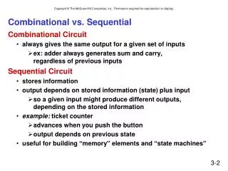
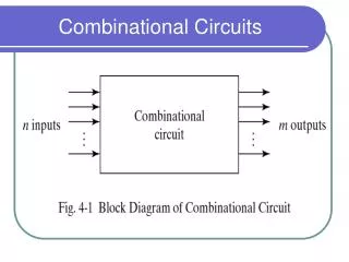
Combinational and Sequential Circuits. Up to now we have discussed combinational circuits. In many cases, one can reduce the complexity of the hardware by using sequential circuits.

E N D
Combinational and Sequential Circuits • Up to now we have discussed combinational circuits. • In many cases, one can reduce the complexity of the hardware by using sequential circuits. • Sequential circuits allow for more flexible and more sophisticated circuit realizations with richer behavior and dynamics.
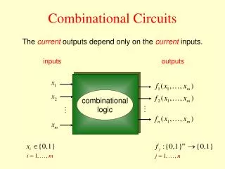
5-1 Sequential circuit block diagram • Combinatorial Logic gives: • Next state functionNext State = f(Inputs, State) • Output function CLOCK Outputs Inputs Combina-tional Logic Next State State (or present state) Storage Elements Synchronous machine
Types of Sequential Circuits t1 t2 t3 t4 t1 t2 t3 t4 • Synchronous • Behavior defined from knowledge of its signals at discrete instances of time • Storage elements observe inputs and can change state only in relation to a timing signal (clock pulses from a clock) • Asynchronous • Behavior defined from knowledge of inputs an any instant of time and the order in continuous time in which inputs change • The synchronous abstraction makes complex designs tractable!
Moore and Mealy Models • Sequential Circuits or Sequential Machines are also called Finite State Machines (FSMs). Two formal models exist: • Moore Model • Named after E.F. Moore • Outputs are only a function of states • Mealy Model • Named after G. Mealy • Outputs are a function of inputs and states
Types of Sequential Circuits Illustra Mealy Comb. logic Outputs Inputs Combina-tional Logic State (or present state) Next State Storage Elements CLOCK • Moore machine: • Outputs = h(State) • Mealy machine • Outputs = g(Inputs, State)
5-2 Storing information: Latches tpd • Use feedback: tpd B=A C= A A Signal B=A appears after a short delay: • How to store information? Reinforces the input A A tpd tpd = propagation delay B tpd C
Latches: Cross-coupled NORs 1 0 1 0 0 1 1 0 1 0 0 B=A=1 0 0 C= A=0 1 1 1 2 2 1 A=0 0 0 • Making the input go to “0” again will memorize the output C=“1” A=0 is memorized How to change contents A from 0 to 1: apply “1” to the first input Set Hold or memory • We have written “1” into the latch: “set” operation
Basic (NOR) S –R Latch R (reset) Q Q S (set) • S R Q Q • 0 0 • 0 1 • 0 • 1 1 0 0 not allowed, unstable (Q=Q) • Function Table: • This element is also the basic building block in SRAM memories hold, no change 0 1 Reset 1 0 Set
Exercise: Basic (NOR) S –R Latch ? ? Stored state unknown S Q 1 Q 2 R • Time sequence behavior: Time R S Q Q Comment 0 0 0 1 1 0 “Set” Q to 1 0 0 1 0 Now Q “remembers” 1 1 0 0 1 “Reset” Q to 0 0 0 0 1 Now Q “remembers” 0 1 1 0 0 Both go low 0 0 ? ? Unstable!
Timing waveforms of NOR S-R latch S Q 1 tpd unstable Q 2 R not allowed S 0 R 0 set 0 Q 1 reset Q No change
Clocked (NOR) S-R Latch S Clk R Q 1 Q 2 • Clk=0: input has no effect: latch is always in “hold” mode • Clk=1: latch is a regular S-R latch
Clocked S - R Latch (continued) S C S R Next state Q(t+1) Q 1 Clock Q 2 R • The Clocked S-R Latch can be described by a table: • The table describeswhat happens after theclock [at time (t+1)]based on: • current inputs (S,R) and • current state Q(t). Q(t) no change • 0 x x • 0 0 • 1 0 1 • 1 1 0 • 1 1 1 Q(t) no change Q(t+1) = 0, Reset Q(t+1) = 1, Set Undefined
Function table of the (NAND) S - R latch S (set) Q Q R (reset) hold, no change 1 0 Set 0 1 Reset 1 1 not allowed, unstable (Q=Q=1) • S = 0, R = 0 is forbidden as input pattern Function table: • S R Q Q • 1 1 • 0 1 • 0 • 0 0
Latch with NAND S S Q C S R Next state Q(t+1) C Q R Q R When both S=R=1: the NAND gates act as inverters and the circuit implements two inverters: “hold mode” Q 1 Q Q Q(t) no change • 0 x x • 0 0 • 1 0 1 • 1 1 0 • 1 1 1 Q(t) no change Q(t+1) = 0, Reset 1 Q(t+1) = 1, Set Q=Q’=1 Undefined 1 A = A A A Clocked latch:
D Latch (Delay latch) D Q C Q Function table D latch: D Q(t+1) 0 0 1 1 D Q Q C • S-R Latch can be usedfor at D Latch: Q(t+1) SR latch: • S R Q+ Q+ • 0 0 hold, • 0 1 01 • 0 10 • 1 1 0 0
Latch issues • Latches can cause serious timing problems (races) in sequential circuits • Due to the fact that a latch is “transparent” when the clock C = 1 • The timing problems can be prevented by using “Flip-Flops”
The Latch Timing Problem (continued) X3 • Similar timing problems in the sequential circuits: Outputs Inputs Combina-tional Logic X2 X2 X1 X1 X1 X0 X2 X1 X0 X2 D Latch (storage) Next State State 1 C=0 • The state should change only once every new clock cycle: • C=1: • Now the current state becomes X1 and a new state is generated by the combinational logic circuit: X2. • However, if C=1, the new “next state” X2 will create a new current state X2!, etc…
How to solve the timing problem: use Flip-Flops C D Q In Q C Out • A solution to the latch timing problem is to break the closed path from In to Out within the storage element Out In Out In D Q C: 0 1 C: 0 1 Q C D-Flip-Flop D-Latch C In Out
S-R Master-Slave Flip-Flop - review Y S S S Q Q Q Q C C C Y’ R R Q R Q • Consists of two clocked S-R latches in series with the clock on the second latch inverted Master Latch Slave Latch C • Master Latch responds to input (Y changes) • Slave latch is inactive: Q unchanged • Master Latch is inactive • Slave latch responds to inputs Y, Y’; • Output Q changes
Symbol: Master-Slave Flip-Flop Y S S S Q Q Q Q C C C Y’ R R Q R Q Notice; the output changes when the clock C goes low. C Symbol: S C R Q Q Sometimes one adds: To indicate that the input responds when C=1, but the output changes when C goes to 0
Timing diagram of a (Nor) S-R Master-Slave Flip-Flop Y S S S Q Q Q Q C C C Y’ R R Q R Q C S R Master out Y S C R 0 Q Slave out Q 0 Q Slave active Master active Output changes at neg. clock edge: Negative edge-trigger FF
Flip-Flop Problem: 1’ catching Y S S S Q Q Q Q C C C Y’ R R Q R Q wrong output should have been 0 Glitch C S R Y Master out Q Slave out Slave active Master active 1’ catching
Flip-Flop Solution: Edge-triggered Positive edge-triggered Negative edge-triggered Clock ignored In The value of the input at the clock transition (negative or positive) determines the output • An edge-triggered flip-flop changes values at the clock edge (transition): • responds to its input at a well-defined moment (at the clock-transition) • ignores the pulse while it is at a constant level
Flip-Flop Solution S S S D Q D S Q Q Q Q Q C C C C R R C C Q R Q Q R Q Q Q • A master-slave D flip-flop which exhibits edge-triggered behavior can be used: • Replacing the first clocked S-R latch with a clocked D latch or • Adding a D input and inverter to a master-slave S-R flip-flop
Edge-Triggered D Flip-Flop D D S Q Q Q C C C Q R Q Q • The 1s-catching behavior is not present with D replacing S and R inputs • The change of the D flip-flop output is associated with the negative edge at the end of the pulse: • It is called a negative-edge triggered flip-flop
No 1’s catching in the edge-triggered D Flip-Flops D D S Q Q Q C C C Q R Q Q no 1’ catching correct output Y C D Y Master out Q Slave active Slave out Master active
Standard Symbols for Storage Elements S S D D R R C C SR D with 1 Control SR (a) Latches S S D D C C R R C C Triggered D Triggered SR Triggered SR (b) Master-Slave Flip-Flops D D C C Triggered D Triggered D (c) Edge-Triggered Flip-Flops • Latches: • Master-Slave:Postponed outputindicators • Edge-Triggered:Dynamicindicator D with 0 Control Triggered D Input samples when C=1 but output changes when C goes 0 Input samples when C=0 but output changes when C goes 1
Timing diagram of a (Nor) S-R Master-Slave Flip-Flop S Q Q Q C R Q = Y S S Q C C Slave active Y’ R R Q Master active Master active C S R S C R Q Y undefined Master out Y’ Q undefined Q undefined Slave out
Direct Inputs S D Q C Q R • At power up or at reset, all or partof a sequential circuit usually isinitialized to a known state beforeit begins operation • This initialization is often doneoutside of the clocked behaviorof the circuit, i.e., asynchronously. • Direct R and/or S inputs that control the state of the latches within the flip-flops are used for this initialization. • For the example flip-flop shown • 0 applied to R resets the flip-flop to the 0 state • 0 applied to S sets the flip-flop to the 1 state
Direct inputs: active-low or active-high Direct inputs • S R C D Q Q’ • 0 1 x x 1 0 • 0 x x 0 1 • 1 1 0 0 1 • 1 1 1 1 0 S D Q C Q R • S R C D Q Q’ • 0 1 x x 0 1 • 0 x x 1 0 • 0 0 0 0 1 • 0 0 1 1 0 S D Q C Q R • D flip-flop with active-low direct inputs : • Active high direct inputs:
Timing Constraints (Section 6.3) 0101101101100110
Flip-Flop Timing: Setup and Hold times – critical time constraints! • Proper operation requires strict timing rules: • Minimum clock pulse width: tw (tWH, tWL) • Set-up time tS: minimum amount of time that the input signal must be present prior to occurrence of the clock transition that causes the output to change • Hold time th: time the input must be kept after the clock transition
Case of Edge triggered Flip-Flop: set-up and hold times tp,max Propagation delay (measured from clock transition): tp,min Out • Negative edge-triggered Out In D Q C Q C C In (D) tS th
Flip-Flop Timing: Setup and Hold times Master-Slave S/R flip-flop (output changes at falling clock): C tS th S/R
Metastability • When one violates the set-up or hold times, the flip-flop can enter a metastable state! • Flip-flops can have three states: • State 0 (Stable) • State 1 (Stable) • Metastable state • Compare to a ball on a hill: After a short, non deterministic time the ball will roll to either state 0 or 1! This will give unpredictable behavior
Metastable behavior metastable • Example of metastable behavior: • After a while the flip-flop will go into a stable state (randomly). • If this happens before the next clock edge, the actual circuits will see a defined input. • The longer the clock period is the less chance of synchronization failure. • Or use two synchronization flip-flops in series Logic 1 (Hi) Logic 0 (Lo) Eventually, the flip-flop will settle (Oscilloscope trace)
Exercise solution • Complete the waveforms below 1st stage active 2nd stage active
Exercise (continued) • Modify this circuit to give a DIRECT (i.e. asynchronous) active-high reset input (make minimal changes to the circuit: add the required reset input)
Exercise - solution • The following timing diagram gives the input and clock for a SR device. Draw the output waveforms assuming the device is (a) clocked D-latch, (b) a Negative edge triggered Master Slave D flip-flop, and (c) a Positive edge triggered D flip-flop. D- Neg. Edge
5-4 Sequential Circuit Analysis • Consider the following circuit: input x A Q D • What does it do? • How do the outputs change when an input arrives? A Q’ C states B Q D CLK Q' C y output
Sequential Circuit Model Mealy Comb. logic Outputs Inputs Combina-tional Logic State (or current state) Storage (D Flip-flops) Next State CLOCK • General Model • Current or Present State at time (t) is stored in an array of flip-flops. • Next Stateis a Boolean function of State and Inputs. • Outputs at time (t) are a Boolean function of State (t) and (sometimes) Inputs (t).
Previous Example (from Fig. 5-15) DA Present state Next State DB • Input: x(t) • Output:y(t) • State: (A(t), B(t)) Example: (AB)= (01), (10) • Next State: (DA(t), DB(t)) = (A(t+1), B(t+1)) Comb. Input logic x A Q D A Q’ C B Q D CLK Q' C y Is this a Moore or Mealy machine? Output logic
Steps for Analyzing a Sequential Circuit • Find the input equations (DA, DB) to the flip-flops (next state equations) and the output equation. • Derive the State Table (describes the behavior of a sequential circuit). • Draw the State Diagram (graphical description of the behavior of the sequential circuit). • Simulation
Step 1: Input and output equations DA x A Q D A Q’ C Next State DB B Q D CLK Q' C y Output • Boolean equations for the inputs to the flip flops: • DA = A(t)x(t)+B(t)x(t) • DB = A(t)x(t) • Output y • y(t) = x(t)(B(t) + A(t)) Present state
Example 1(from Fig. 5-15) (continued) 1 0 1 0 0 0 1 0 • Where in time are inputs, outputs and states defined?
Step 2: State Table Characteristics • The state table: shows what the next state and the output will be as a function of the present state and the input: • The State Table can be considered a truth table defining the combinational circuits: • the inputs are Present State, Input, • and the outputs are Next State and Output Present State Input Next State Output Outputsof the table Inputs of the combinational circuit
State Table Inputs of the table Outputs of the table Present State Input Next State Output A(t) B(t) x(t) A(t+1) B(t+1) y(t) 0 0 0 0 0 1 23rows (2m+n) rows 0 1 0 0 1 1 1 0 0 1 0 1 m: no. of FF n: no. of inputs 1 1 0 1 1 1 • For the example: A(t+1) = A(t)x(t) + B(t)x(t) B(t+1) =A (t)x(t) y(t) =x (t)(B(t) + A(t)) 0 0 0 0 1 0 0 0 1 1 1 0 0 0 1 1 0 0 0 0 1 1 0 0
Alternate State Table Present Next State Output State x(t)=0 x(t)=1 x(t)=0 x(t)=1 A(t) B(t) A(t+1)B(t+1) A(t+1)B(t+1) y(t) y(t) 0 0 0 0 0 1 0 0 0 1 0 0 1 1 1 0 2m 1 0 0 0 1 0 1 0 1 1 0 0 1 0 1 0 • The previous (1-dimensional table) can become quite lengthy with 2m+n rows (m=no. of FF; n=no. of inputs) • Alternatively, a 2-dimensional table has the present state in the left column and inputs across the top row • A(t+1) = A(t)x(t) + B(t)x(t) • B(t+1) =A (t)x(t) • y(t) =x (t)(B(t) + A(t))