Download
1 / 56
580 likes | 715 Vues
Circuiti Logici. f. x 1. . x 2. f(x 1 ,x 2 ) = x 1 +x 2 = x 1 x 2. OR. Proprietà della funzione OR. Commutativa:. x 1 + x 2 = x 2 + x 1. Estesa a più variabili. x 1 + x 2 + x 3 + … + x n = 1 se x i = 1 (i=1,…,n). Associativa:.

E N D
Circuiti Logici
f x1 x2 f(x1,x2) = x1+x2 = x1 x2 OR
Proprietà della funzione OR Commutativa: x1 + x2 = x2 + x1 Estesa a più variabili x1 + x2 + x3 + … + xn = 1 se xi = 1 (i=1,…,n) Associativa: (x1 + x2 )+ x3 = x1 + (x2 + x3) Inoltre: 0 + x = x 1 + x = 1
f x1 x2 f(x1,x2) = x1•x2 = x1 x2 AND
Proprietà della funzione AND Commutativa: x1• x2 = x2• x1 Estesa a più variabili x1• x2• x3• … • xn = 1 xi = 1 (i=1,…,n) Associativa: (x1• x2 ) • x3 = x1 • (x2• x3) Inoltre: 0 • x = 0 1 • x = x
f 1 1 x1 x2 f(x1,x2) = x1 x2 Exclusive OR
Proprietà della funzione Exclusive OR Commutativa: x1 x2 = x2 x1 Estesa a più variabili x1 x2 x3 … xn = 1 se xi = 1 e xk = 0 ik (i,k=1,…,n) (x1 x2 ) x3 = x1 (x2 x3) Associativa: 0 x = x 1 x = x Inoltre:
f 1 x1 f(x) = x NOT
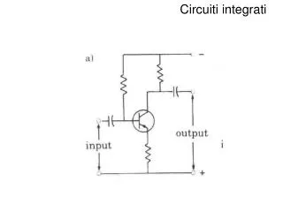
V alimentazione Transistor Bipolare (BJT) resistenza base V uscita collettore V ingresso emettitore V massa V ingresso < Vlim V uscita = V alim. V ingresso > Vlim V uscita = Vmassa
AND x2 V f y x1
V OR y f x1 z x2
Tecnologie microelettroniche Transistor bipolari (o a giunzione) o Transistor BJT (Bipolar Junction Transistor) Tecnologia TTL (Transistor Transistor Logic) Tecnologia ECL ( Emitter Couple Logic) Transistor ad effetto di inversione o Transistor MOS (Metal Oxide Semiconductor) Tecnologia CMOS (Complementary Metal Oxide Semiconductor)
Simboli standard per porte logiche x1 OR x1 + x2 x2 x1 AND x1• x2 x2 NOT x x x1 EX-OR x1 x2 x2
x1 x2 f f = x1• x2 + x1 •x2
x1 x2 f x3 f = x1x2 + x2 x3
Minimizzazione di funzioni logiche OR AND Commutativa x+y=y+x xy=yx Associativa (x+y)+z=x+(y+z) (xy)z=x(yz) Distributiva x+yz=(x+y)(x+z) x(y+z)=xy+xz Idempotenza x+x=x xx=x Involuzione x = x x +x= 1 Complemento xx= 0 x+y =xy De Morgan xy =x +y 1+x=1 0 x=0 0+x=x 1 x=x
Minimizzazione di funzioni logiche f = x1x2x3 + x1x2 x3 +x1 x2x3 + x1x2x3 + x1x2 x3
x1x2 x3 00 01 11 10 Mappa di Karnaugh 0 1
Minimizzazione di funzioni logiche x1x2 x3 00 01 11 10 0 1 x1x2 x2 x3 f =x1x2 + x2 x3
x1x2 x3 00 01 11 10 0 1
Minimizzazione di funzioni logiche x1x2 x3 00 01 11 10 0 1 x2 x1 x3 f =x2 + x1x3
x1x2 00 01 11 10 x3x4 00 01 11 10 x1x4 x2 x3 x4 f =x2 x3 x4+ x1x4
x1x2 00 01 11 10 x3x4 00 01 11 10 x2x3 x4 x2x4 x1x3 f = x2x4 + x1x3 + x2x3 x4
x1x2 00 01 11 10 x3x4 00 01 11 10 x4 x2x3 f =x4+ x2x3
x1x2 00 01 11 10 x3x4 00 01 11 10 x1x2x3 x2x3x4
x1x2 00 01 11 10 x3x4 00 01 11 10 x1x2x3 x2x3x4 x1x3 x4
x1x2 00 01 11 10 x3x4 00 01 11 10 x1x2x3 x2x3x4 x1 x2 x4
Altre Porte logiche x1 x1 x2 NAND x2
Altre Porte logiche x1 x1 x2 NOR x2
Proprietà x1 x2 = x1x2= x1 +x2 x1 x2 = x1+x2= x1x2 x1 x2 … xn = x1x2 … xn= x1 +x2 +…+ xn x1 x2 … xn = x1+x2+ …+ xn = x1x2 … xn Non vale la proprietà associativa
Circuiti logici solo con porte NAND (x1 x2 ) (x3 x4 ) = (x1 x2 ) (x3 x4 ) = x1 x2 + x3 x4 = x1 x2 + x3 x4 x1 x1 x2 x2 x3 x3 x4 x4
Associatività Associativa (x+y)+z=x+(y+z) (xy)z=x(yz) x1 x2 x3 x1 x2 x3
Non Associatività x1 x2 x3 x1 x2 x3
Realizzazione di Porte Logiche Nei circuiti elettronici per rappresentare le variabili logiche Sono utilizzati sia livelli di tensione che di corrente Per stabilire una corrispondenza tra livelli di tensione e valori logici si usa una soglia (threshold) Vmax V1 Soglia V0 Vmin
Vs Vs NOT R Vout Vout Vin Vin V0 Vout > V1 Vin V1 Vout < V0
NAND x2 V V f y x1 f x2 AND x1
V y V f x1 z f x2 x1 x2 NOR OR
Criteri per la realizzazione di P.L. Velocità ( Ritardo di propagazione e tempo di transizione) Potenza Densità di packaging Immunità al rumore Caratteristica di carico fan-in Capacità di carico fan-out
Definizione di Circuiti Circuiti il cui stato dipende solo dagli ingressi Circuiti Combinatori Circuiti il cui stato dipende non solo dagli ingressi ma dalle configurazioni precedenti Circuiti Sequenziali
Memorie: Bistabile (Flip-Flop) R Qa Qb S Bistabile RS
Memorie: Bistabile (Flip-Flop) 1 R 0 1 S 0 1 Qa 0 1 Qb 0
Bistabile Sincroni R Qa Cl Qb S
Memorie: Bistabile Sincrono 1 S 0 1 R 0 1 Cl 0 1 Qa 0 1 Qb 0
Bistabile Sincroni R Qa Cl Qb S D Bistabile D
Altri Bistabili RS Master-Slave (Bistabili JK) Edge-Triggered (Bistabili D) Bistabili JK S=JQ R=KQ
Shift Register F2 F3 F4 F1 Out In J Q J Q J Q J Q K Q K Q K Q K Q Cl
Shift Register F2 F3 F4 F1 J Q J Q J Q J Q K Q K Q K Q K Q Clock In Shift/ Load
Contatori F2 F3 F4 F1 J Q J Q J Q J Q Cl K Q K Q K Q K Q 1 Ripple