Download
1 / 1
10 likes | 134 Vues
Three-dimensional TiO 2 nanotube arrays for photo-device application. Ahmed Al-Haddad 1,2,3 , Yaoguo Fang 1,2 , Huaping Zhao 1,2 , Yong Lei 1,2

E N D
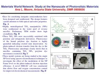
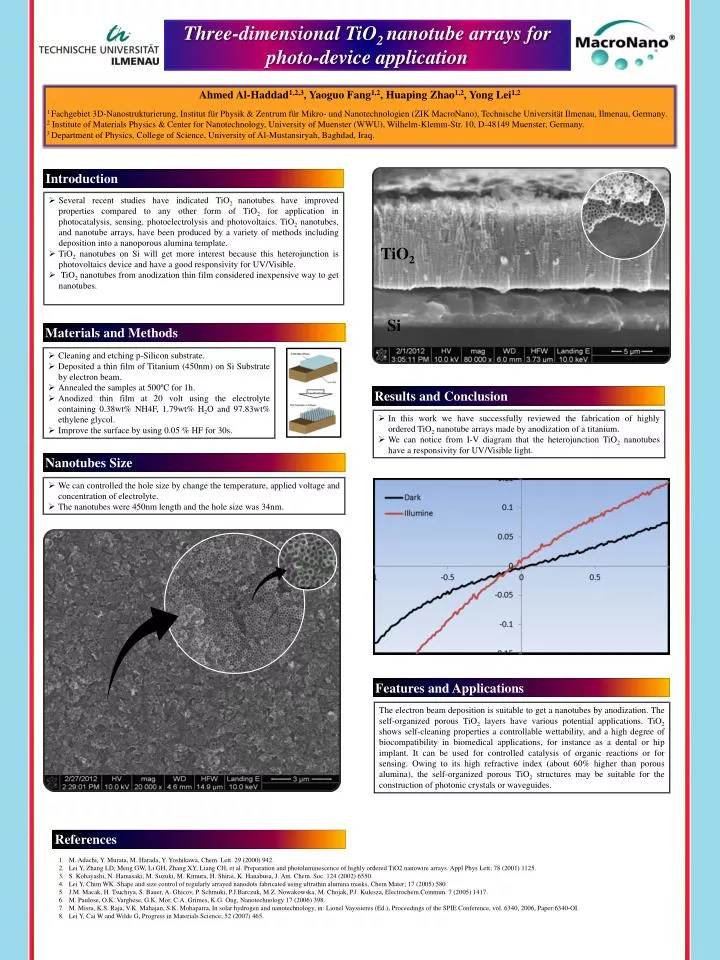
Three-dimensional TiO2 nanotube arrays for photo-device application Ahmed Al-Haddad1,2,3, YaoguoFang1,2, HuapingZhao1,2, Yong Lei1,2 1 Fachgebiet 3D-Nanostrukturierung, Institut für Physik & Zentrum für Mikro- und Nanotechnologien (ZIK MacroNano), Technische Universität Ilmenau, Ilmenau, Germany. 2 Institute of Materials Physics & Center for Nanotechnology, University of Muenster (WWU), Wilhelm-Klemm-Str. 10, D-48149 Muenster, Germany. 3 Department of Physics, College of Science, University of Al-Mustansiryah, Baghdad, Iraq. Nanotubes Size • We can controlled the hole size by change the temperature, applied voltage and concentration of electrolyte. • The nanotubes were 450nm length and the hole size was 34nm. Introduction • Several recent studies have indicated TiO2 nanotubes have improved properties compared to any other form of TiO2 for application in photocatalysis, sensing, photoelectrolysisand photovoltaics. TiO2nanotubes, and nanotube arrays, have been produced by a variety of methods including deposition into a nanoporous alumina template. • TiO2 nanotubes on Si will get more interest because this heterojunction is photovoltaics device and have a good responsivity for UV/Visible. • TiO2nanotubes from anodization thin film considered inexpensive way to get nanotubes. TiO2 Features and Applications Results and Conclusion References The electron beam deposition is suitable to get a nanotubes by anodization. The self-organized porous TiO2 layers have various potential applications. TiO2shows self-cleaning properties a controllable wettability, and a high degree of biocompatibility in biomedical applications, for instance as a dental or hip implant. It can be used for controlled catalysis of organic reactions or for sensing. Owing to its high refractive index (about 60% higher than porous alumina), the self-organized porous TiO2 structures may be suitable for the construction of photonic crystals or waveguides. • In this work we have successfully reviewed the fabrication of highly ordered TiO2nanotube arrays made by anodization of a titanium. • We can notice from I-V diagram that the heterojunction TiO2nanotubes have a responsivity for UV/Visible light. M. Adachi, Y. Murata, M. Harada, Y. Yoshikawa, Chem. Lett. 29 (2000) 942. Lei Y, Zhang LD, Meng GW, Li GH, Zhang XY, Liang CH, et al. Preparation and photoluminescence of highly ordered TiO2 nanowire arrays. ApplPhysLett; 78 (2001) 1125. S. Kobayashi, N. Hamasaki, M. Suzuki, M. Kimura, H. Shirai, K. Hanabusa, J. Am. Chem. Soc. 124 (2002) 6550. Lei Y, Chim WK. Shape and size control of regularly arrayed nanodots fabricated using ultrathin alumina masks, Chem Mater; 17 (2005) 580. J.M. Macak, H. Tsuchiya, S. Bauer, A. Ghicov, P. Schmuki, P.J.Barczuk, M.Z. Nowakowska, M. Chojak, P.J. Kulesza, Electrochem.Commun. 7 (2005) 1417. M. Paulose, O.K. Varghese, G.K. Mor, C.A. Grimes, K.G. Ong, Nanotechnology 17 (2006) 398. M. Misra, K.S. Raja, V.K. Mahajan, S.K. Mohapatra, In solar hydrogen and nanotechnology, in: Lionel Vayssieres (Ed.), Proceedings of the SPIE Conference, vol. 6340, 2006, Paper:6340-OI. Lei Y, Cai W and Wilde G, Progress in Materials Science; 52 (2007) 465. Si Materials and Methods • Cleaning and etching p-Silicon substrate. • Deposited a thin film of Titanium (450nm) on Si Substrate by electron beam. • Annealed the samples at 500ºC for 1h. • Anodized thin film at 20 volt using the electrolyte containing 0.38wt% NH4F, 1.79wt% H2O and 97.83wt% ethylene glycol. • Improve the surface by using 0.05 % HF for 30s.