Download
1 / 59
590 likes | 762 Vues
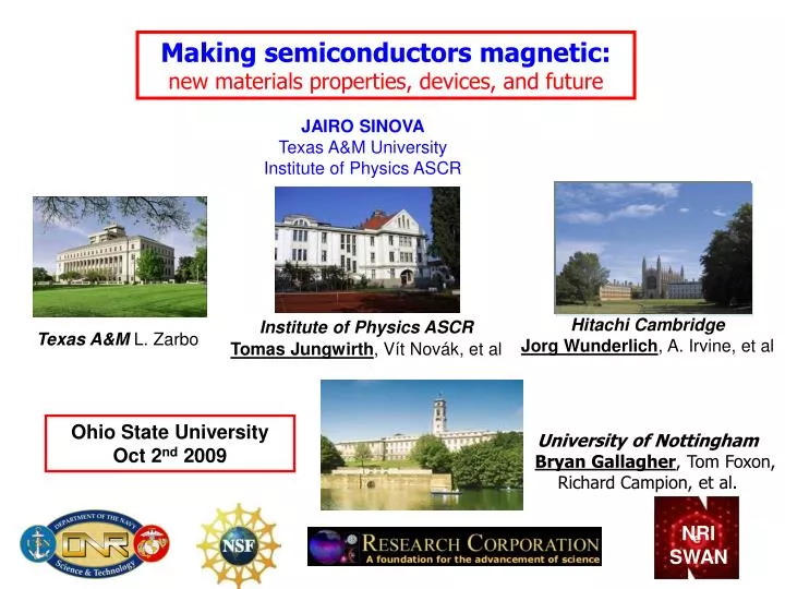
NRI SWAN. Making semiconductors magnetic: new materials properties, devices, and future. JAIRO SINOVA Texas A&M University Institute of Physics ASCR. Hitachi Cambridge Jorg Wunderlich , A. Irvine, et al. Institute of Physics ASCR Tomas Jungwirth , Vít Novák, et al.

E N D
NRI SWAN Making semiconductors magnetic: new materials properties, devices, and future JAIRO SINOVA Texas A&M University Institute of Physics ASCR Hitachi Cambridge Jorg Wunderlich, A. Irvine,et al Institute of Physics ASCR Tomas Jungwirth, Vít Novák, et al Texas A&ML. Zarbo Ohio State University Oct 2nd 2009 University of Nottingham Bryan Gallagher, Tom Foxon,Richard Campion, et al.
OUTLINE • Motivation • Ferromagnetic semiconductor materials: • (Ga,Mn)As - general picture • Growth, physical limits on Tc • Related FS materials (searching for room temperature) • Understanding critical behavior in transport • Ferromagnetic semiconductors & spintronics • Tunneling anisotropic magnetoresistive device • Transistors (4 types)
ENGINEERING OF QUANTUM MATERIALS Technologically motivated and scientifically fueled • Generates new physics: • Tunneling AMR • Coulomb blockade AMR • Nanostructure magnetic anisotropy engineering Incorporate magnetic properties with semiconductor tunability (MRAM, etc) • Understanding complex phenomena: • Spherical cow of ferromagnetic systems (still very complicated) • Engineered control of collective phenomena More knobs than usual in semiconductors: density, strain, chemistry/pressure, SO coupling engineering
Ferromagnetic semiconductor research : strategies • Create a material that marriages the tunability of semiconductors and the collective behavior of ferromagnets; once created search for room temperature systems • Study new effects in this new material and utilize in metal-based spintronics • Develop a three-terminal gated spintronic device to progress from sensors & memories to transistors & logic
(Ga,Mn)As GENERAL PICTURE
Ga Mn As Mn Ferromagnetic semiconductors Need true FSs not FM inclusions in SCs GaAs - standard III-V semiconductor Group-II Mn - dilute magnetic moments & holes (Ga,Mn)As - ferromagnetic semiconductor +
Ga As Mn What happens when a Mn is placed in Ga sites: Mn–hole spin-spin interaction As-p 5 d-electrons with L=0 S=5/2 local moment intermediate acceptor (110 meV) hole Mn-d hybridization Hybridization like-spin level repulsion Jpd SMn shole interaction In addition to the Kinetic-exchange coupling, for a single Mn ion, the coulomb interaction gives a trapped hole (polaron) which resides just above the valence band
Ga Ga Mn As As Mn Mn Transition to a ferromagnet when Mn concentration increases GaAs:Mn – extrinsic p-type semiconductor EF spin ~1% Mn << 1% Mn >2% Mn DOS Energy spin onset of ferromagnetism near MIT As-p-like holes localized on Mn acceptors valence band As-p-like holes Ga Mn As Mn FM due to p-d hybridization (Zener local-itinerant kinetic-exchange)
(Ga,Mn)As GROWTH high-T growth • Low-T MBE to avoid precipitation • High enough T to maintain 2D growth • need to optimize T & stoichiometry • for eachMn-doping • Inevitable formation of interstitial Mn-double-donors compensating holes and moments • need to anneal out but without loosing MnGa optimal-T growth
Interstitial Mn out-diffusion limited by surface-oxide Polyscrystalline 20% shorter bonds O GaMnAs-oxide x-ray photoemission MnI++ GaMnAs Olejnik et al, ‘08 10x shorther annealing with etch Optimizing annealing-T another key factor Rushforth et al, ‘08
(Ga,Mn)As GENERAL THEORY
HOW DOES ONE GO ABOUT UNDERSTANDING SUCH SYSTEMS • One could solve the full many body S.E.: not possible AND not fun • Combining phenomenological models (low degrees of freedom) and approximations and comparison to other computational technieques while checking against experiments “This is the art of condensed matter science, an intricate tango between theory and experiment whose conclusion can only be guessed at while the dance is in progress” A.H.M et al., in “Electronic Structure and Magnetism in Complex Materials” (2002).
Theoretical Approaches to DMSs Jungwirth, Sinova, Masek, Kucera, MacDonald, Rev. of Mod. Phys. 78, 809 (2006) • First Principles LSDA PROS: No initial assumptions, effective Heisenberg model can be extracted, good for determining chemical trends CONS:Size limitation, difficulty dealing with long range interactions, lack of quantitative predictability, neglects SO coupling (usually) • Microscopic TB models PROS: “Unbiased” microscopic approach, correct capture of band structure and hybridization, treats disorder microscopically (combined with CPA), very good agreement with LDA+U calculations CONS: neglects (usually) coulomb interaction effects, difficult to capture non-tabulated chemical trends, hard to reach large system sizes • k.p Local Moment PROS:simplicity of description, lots of computational ability, SO coupling can be incorporated, CONS: applicable only for metallic weakly hybridized systems (e.g. optimally doped GaMnAs), over simplicity (e.g. constant Jpd), no good for deep impurity levels (e.g. GaMnN)
Magnetism in systems with coupled dilute moments and delocalized band electrons coupling strength / Fermi energy band-electron density / local-moment density (Ga,Mn)As
Impurity bandit vs Valence Joe KP Eastwood Fast principles Jack Which theory is right?
How well do we understand (Ga,Mn)As? In the metallic optimally doped regime GaMnAs is well described by a disordered-valence band picture: both dc-data and ac-data are consistent with this scenario. The effective Hamiltonian (MF) and weak scattering theory (no free parameters) describe (III,Mn)V metallic DMSs very well in the optimally annealed regime: • Ferromagnetic transition temperatures • Magneto-crystalline anisotropy and coercively • Domain structure • Anisotropic magneto-resistance • Anomalous Hall effect • MO in the visible range • Non-Drude peak in longitudinal ac-conductivity • Ferromagnetic resonance • Domain wall resistance • TAMR • Transport critical behaviour • Infrared MO effects TB+CPA and LDA+U/SIC-LSDA calculations describe well chemical trends, impurity formation energies, lattice constant variations upon doping
Mn Mn Mn As Ga Problems for GaMnAs (late 2002) • Curie temperature limited to ~110K. • Only metallic for ~3% to 6% Mn • High degree of compensation • Unusual magnetization (temperature dep.) • Significant magnetization deficit “110K could be a fundamental limit on TC” But are these intrinsic properties of GaMnAs ??
Can a dilute moment ferromagnet have a high Curie temperature ? EXAMPLE OF THE PHYSICS TANGO • The questions that we need to answer are: • Is there an intrinsic limit in the theory models (from the physics of the phase diagram) ? • Is there an extrinsic limit from the ability to create the material and its growth (prevents one to reach the optimal spot in the phase diagram)?
Intrinsic properties of (Ga,Mn)As COMBINATION OF THEORY APPROACHES PREDICTS: Tc linear in MnGa local moment concentration; falls rapidly with decreasing hole density in more than 50% compensated samples; nearly independent of hole density for compensation < 50%. Jungwirth, Wang, et al. Phys. Rev. B 72, 165204 (2005)
Extrinsic effects: Interstitial Mn - a magnetism killer Mn As Interstitial Mn is detrimental to magnetic order: compensating double-donor – reduces carrier density couples antiferromagnetically to substitutional Mneven in low compensation samplesBlinowski PRB ‘03, Mašek, Máca PRB '03 Yu et al., PRB ’02: ~10-20% of total Mn concentration is incorporated as interstitials Increased TC on annealing corresponds to removal of these defects.
MnGa and MnI partial concentrations As grown Materials calculation Jungwirth, Wang, et al. Phys. Rev. B 72, 165204 (2005) Microscopic defect formation energy calculations: No signs of saturation in the dependence of MnGa concentration on total Mn doping
Experimental hole densities: measured by ordinary Hall effect Open symbols & half closed as grown. Closed symbols annealed Low Compensation Obtain Mnsub assuming change in hole density due to Mn out diffusion High compensation Jungwirth, Wang, et al. Phys. Rev. B 72, 165204 (2005) Annealing can vary significantly increases hole densities.
Mnsub MnInt Obtain Mnsub & MnInt assuming change in hole density due to Mn out diffusion Experimental partial concentrations of MnGa and MnI in as grown samples Theoretical linear dependence of Mnsub on total Mn confirmed experimentally Jungwirth, Wang, et al. Phys. Rev. B 72, 165204 (2005) SIMS: measures total Mn concentration. Interstitials only compensation assumed
Can we have high Tc in Diluted Magnetic Semicondcutors? NO INTRINSIC LIMIT NO EXTRINSIC LIMIT Tc linear in MnGa local (uncompensated) moment concentration; falls rapidly with decreasing hole density in heavily compensated samples. There is no observable limit to the amount of substitutional Mn we can put in Define Mneff = Mnsub-MnInt
Linear increase of Tc with Mneff = Mnsub-MnInt High compensation 8% Mn Tc as grown and annealed samples Open symbols as grown. Closed symbols annealed • Concentration of uncompensated MnGa moments has to reach ~10%. Only 6.2% in the current record Tc=173K sample • Charge compensation not so important unless > 40% • No indication from theory or experiment that the problem is other than technological - better control of growth-T, stoichiometry
188K!! Tc limit in (Ga,Mn)As remains open 2008 Olejnik et al “... Ohno’s ‘98 Tc=110 K is the fundamental upper limit ..” Yu et al. ‘03 “…Tc =150-165 K independent of xMn>10% contradicting Zener kinetic exchange ...” Mack et al. ‘08 ` “Combinatorial” approach to growth with fixed growth and annealing T’s
Getting to higher Tc: Strategy A - Effective concentration of uncompensated MnGa moments has to increase beyond 6% of the current record Tc=173K sample. A factor of 2 needed 12% Mn would still be a DMS - Low solubility of group-II Mn in III-V-host GaAs makes growth difficult Low-temperature MBE Strategy A:stick to (Ga,Mn)As - alternative growth modes (i.e. with proper substrate/interface material) allowing for larger and still uniform incorporation of Mn in zincblende GaAs More Mn - problem with solubility
Getting to higher Tc: Strategy B • Find DMS system as closely related to (Ga,Mn)As as possible with • larger hole-Mn spin-spin interaction • lower tendency to self-compensation by interstitial Mn • larger Mn solubility • independent control of local-moment and carrier doping (p- & n-type)
Other (III,Mn)V’s DMSs Kudrnovsky et al. PRB 07 Delocalized holes long-range coupl. Weak hybrid. Mean-field but low TcMF InSb d5 Impurity-band holes short-range coupl. Strong hybrid. Large TcMF but low stiffness GaP (Al,Ga,In)(As,P) good candidates, GaAs seems close to the optimal III-V host
Steps so far in strategy B: • larger hole-Mn spin-spin interaction : DONE BUT DANGER IN PHASE DIAGRAM • lower tendency to self-compensation by interstitial Mn: DONE • larger Mn solubility ? • independent control of local-moment and carrier doping (p- & n-type)? Using DEEP mathematics to find a new material 3=1+2
EF L As p-orb. Ga s-orb. As p-orb. III = I + II Ga = Li + Zn GaAs and LiZnAs are twin SC LDA+U says that Mn-doped are also twin DMSs It can be n and p doped!!! No solubility limit for group-II Mn substituting for group-II Zn !!!! Masek, et al. PRB (2006)
Towards spintronics in (Ga,Mn)As: FM & transport Dilute-moment MS F~ d- Dense-moment MS F<< d- Eu - chalcogenides Broad peak near Tc disappeares with annealing (higher uniformity)??? Critical contribution to resistivity at Tc ~ magnetic susceptibility
When density of carriers is smaller than density of local moments what matters is the long range behavior of Γ (which goes as susceptibility) When density of carriers is similar to density of local moments what matters is the short range behavior of Γ (which goes as the energy) Tc Ni EuCdSe Tc
d/dT singularity at Tc – consistent with kF~d- Annealing sequence Optimized materials with x=4-12.5% and Tc=80-185K Remarkably universal both below and above Tc V. Novak, et al “Singularity in temperature derivative of resistivity in (Ga,Mn)As at the Curie point”, Phys. Rev. Lett. 101, 077201 (2008).
OUTLINE • Motivation • Ferromagnetic semiconductor materials: • (Ga,Mn)As - general picture • Growth, physical limits on Tc • Related FS materials (searching for room temperature) • Understanding critical behavior in transport • Ferromagnetic semiconductors & spintronics • Tunneling anisotropic magnetoresistive device • Transistors (4 types)
Au AMR TMR ~ 1% MR effect ~ 100% MR effect Exchange split & SO-coupled bands: TAMR Exchange split bands: discovered in (Ga,Mn)As Gold et al. PRL’04
TAMR in metal structures experiment Park, et al, PRL '08 ab intio theory Shick, et al, PRB '06, Park, et al, PRL '08 Also studied by Parkin et al., Weiss et al., etc.
Gating of highly doped (Ga,Mn)As: p-n junction FET (Ga,Mn)As/AlOx FET with large gate voltages, Chiba et al. ‘06 p-n junction depletion estimates ~25% depletion feasible at low voltages Olejnik et al., ‘08
Increasing and decreasing AMR and Tc with depletion Tc Tc AMR
Persistent variations of magnetic properties with ferroelectric gates Stolichnov et al., Nat. Mat.‘08
Electro-mechanical gating with piezo-stressors Strain & SO Rushforth et al., ‘08 Electrically controlled magnetic anisotropies via strain
(Ga,Mn)As spintronic single-electron transistor Wunderlich et al. PRL ‘06 Huge, gatable, and hysteretic MR Single-electron transistor Two "gates": electric and magnetic
Single-electron charging energy controlled by Vg and M M [010] [110] F Q VD [100] Source Drain [110] [010] Gate VG Q0 Q0 e2/2C magnetic electric & SO-coupling (M) control of Coulomb blockade oscillations Theory confirms chemical potential anisotropies in (Ga,Mn)As & predicts CBAMR in SO-coupled room-Tc metal FMs
V DD V V A B V B V A Nonvolatile programmable logic 1 0 ON OFF Variant p- or n-type FET-like transistor in one single nano-sized CBAMR device 1 0 ON OFF 1 1 0 0 0 1 1 0 OFF ON OFF ON ON OFF ON 0 1 1 1 0 0 1 1 Vout A B Vout 0 0 0 1 0 1 0 1 1 1 1 1 OFF ON OFF 1 1 0 0 “OR” OFF ON OFF ON
V DD V V A B V B V A Nonvolatile programmable logic 1 0 ON OFF Variant p- or n-type FET-like transistor in one single nano-sized CBAMR device 1 0 ON OFF Vout A B Vout 0 0 0 1 0 1 0 1 1 1 1 1 “OR”
Device design Physics of SO & exchange Materials FSs and metal FS with strong SO Chemical potential CBAMR SET FSs Tunneling DOS TAMR Tunneling device metal FMs Group velocity & lifetime AMR Resistor