Download
1 / 3
30 likes | 210 Vues
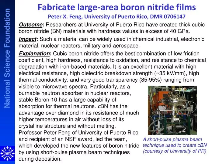
Fabricate large-area boron nitride films Peter X. Feng, University of Puerto Rico, DMR 0706147. Outcome : Researchers at University of Puerto Rico have created thick cubic boron nitride (BN) materials with hardness values in excess of 40 GPa.

E N D
Fabricate large-area boron nitride films Peter X. Feng, University of Puerto Rico, DMR 0706147 Outcome: Researchers at University of Puerto Rico have created thick cubic boron nitride (BN) materials with hardness values in excess of 40 GPa. Impact: Such a material can be widely used in chemical industrial, electronic material, nuclear reactors, military and aerospace. Explanation:Cubic boron nitride offers the best combination of low friction coefficient, high hardness, resistance to oxidation, and resistance to chemical degradation with iron-based materials. It is an excellent material with high electrical resistance, high dielectric breakdown strength (~35 kV/mm), high thermal conductivity, and very good transparency (85-95%) ranging from visible to microwave spectra. Particularly, as a burnable neutron absorber in nuclear reactors, stable Boron-10 has a large capability of absorption for thermal neutrons. cBN has the advantage over diamond in its resistance of much higher temperatures in air without loss of its crystalline structure and without melting. Professor Peter Feng of University of Puerto Rico and recipient of an NSF award, led the team, which developed the new features of boron nitride by using short-pulse plasma beam techniques during deposition. A short-pulse plasma beam technique used to create cBN (courtesy of University of PR)
Fabricate large-area boron nitride films Peter X. Feng, University of Puerto Rico, DMR 0706147 Thick, flat and high transparent c-BN films were successfully synthesized on Si and Mo substrates using pulse plasma deposition technique. The thickness of the films prepared at 400 0C and 600 0C were nearly same (around 3 µm), indicating that the growth rate at the present temperatures was similar. From experimental results, it could be concluded that types of the substrates did not affect BN crystalline structures by much. However, temperature has an obvious effect i.e. low substrate temperature of deposition produced less content of c-BN (111) phase inside the sample, whereas, the sp3 content increased with the increased substrate temperature. This change indicates the evolution of the crystalline structure from h-BN to c-BN domination inside the sample following an increase of substrate temperature. SEM micrographs of BN films prepared on Si substrates (a) at 400 0C and (b) at 600 0C.
Fabricate large-area boron nitride films Peter X. Feng, University of Puerto Rico, DMR 0706147 The researchers also spent a significant part of their time for educational activities. It includes visiting local schools, giving talks and demonstrations. For example, they visited and gave talks or demonstrations to four different high schools and one primary school of students in last year. The research team also hosted 5 students from 4 different high schools for two weeks of internship in research laboratory as shown in Figure. The subjects of these modules have far included general physics. Educational visits and talks to the high school students during internship A stress is on student involvement and learning through exploration of concepts and ideas.Through hands-on approach, and attendance of joint group meetings, students have an opportunity to ask questions, and gain insight into how different fields of scientists work together toward a common goal. Students working with those from different but related disciplines would learn the value of cross-disciplinary approaches. All these approaches greatly raise students’ interests in ceramic material research.