Download
1 / 42
630 likes | 1.11k Vues
http://emalwww.engin.umich.edu/education_materials/microscopy.html. A Question from Last Year Final Exam.

E N D
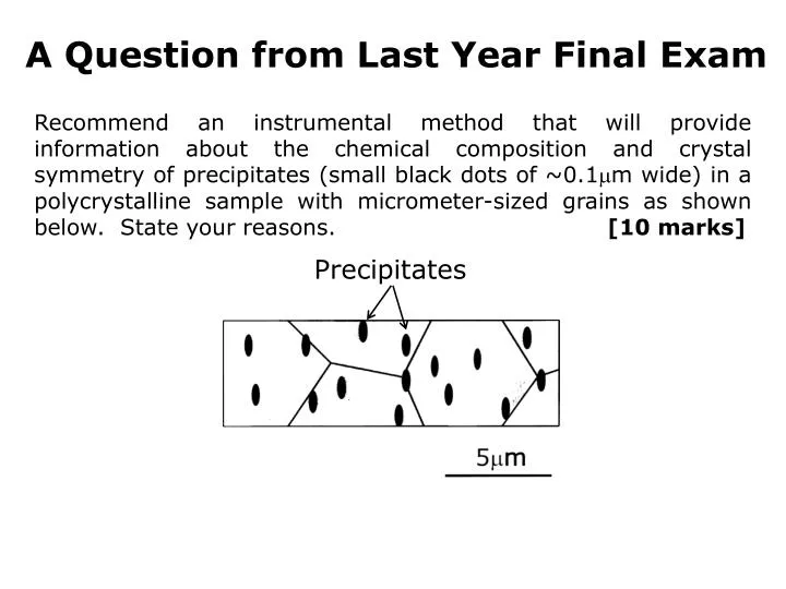
http://emalwww.engin.umich.edu/education_materials/microscopy.htmlhttp://emalwww.engin.umich.edu/education_materials/microscopy.html A Question from Last Year Final Exam Recommend an instrumental method that will provide information about the chemical composition and crystal symmetry of precipitates (small black dots of ~0.1m wide) in a polycrystalline sample with micrometer-sized grains as shown below. State your reasons. [10 marks] Precipitates http://www.youtube.com/watch?v=yqLlgIaz1L0 see atoms by TEM
G.B. NN Limits of OM, SEM, SPM and XRD core G.B. NN shell BT BT BT-BaTiO3 NN-NaNbO3 G.B.-Grain boundary M.G.J.-multiple grain junction M.G.J. EDS 0.2m NN/BT • Lateral resolution: ~m • Details of microstructure: e.g., domain structure, chemical inhomogeneity phase distribution, grain boundaries, interfaces, precipitates, dislocations, etc.
Chemical analysis at a nanometer scale in a Transmission Electron Microscope (TEM)
Why TEM? The uniqueness of TEM is the ability to obtain full morphological (grain size, grain boundary and interface, secondary phase and distribution, defects and their nature, etc.), crystallographic, atomic structural and microanalytical such as chemical composition (at nm scale), bonding (distance and angle), electronic structure, coordination number data from the sample. TEM is the most efficient and versatile technique for the characterization of materials. http://www.youtube.com/watch?v=yqLlgIaz1L0 see atoms by TEM
Lecture-6 Transmission Electron Microscopy (TEM)Scanning Transmission Electron Microscopy (STEM) • What is a TEM? • How it works - gun, lenses, specimen holder • Resolution • What can a TEM do? • Imaging and diffraction Imaging-diffraction and phase contrast Diffraction-Selected area electron diffraction (SAED) and Convergent beam electron diffraction (CBED) • Chemical analysis EDS, Electron Energy Loss Spectroscopy (EELS) Energy Filtered Imaging http://emalwww.engin.umich.edu/education_materials/microscopy.html http://www.youtube.com/watch?v=6fX1m2rImiM to~2:40 History & applications
What is TEM? Lecture-6 Transmission Electron Microscopy (TEM)Scanning Transmission Electron Microscopy (STEM) • TEM is an microscopy technique that functions similar to a light microscope, which uses a beam of exited electrons as a light source to provide mophorlogical, compositional and crystallographic information of an ultra thin specimen. • The image is formed by the interaction of the electrons transmitted through the specimen, which is then magnified and focused on a fluorescence screen containing a layer of photographic film. • What is a TEM? • How it works - gun, lenses, specimen stage • Resolution http://www.youtube.com/watch?v=fxEVsnZT8L8 ~2:20-2:40 fluorescence screen http://www.youtube.com/watch?v=C3uU8c376Aw&list=PLIRAzwu_npNcnPGi2sOk2aaNaS3vzU-N1 Milestones of Science: Ernst Ruska and the Electron Microscope at~5:00-7:15 and ~9:03-9:23
Comparison of OM and TEM Principal features of an optical microscope and a transmission electron microscope, drawn to emphasize the similarities of overall design.
http://www.youtube.com/watch?v=fToTFjwUc5M Structure and Function of TEM CM200 (200kV) Column Electron Gun EDS Detector Condenser Lens Objective Lens Specimen Holder SAD Aperture Binocular Magnifying Lenses TV Monitor Camera Chamber Viewing Chamber Cost: $4,000,000 http://www.youtube.com/watch?v=6fX1m2rImiM at~2:40-4:40 http://www.youtube.com/watch?v=2wEmsDh_l_A at~0:30
Vacuum The electron microscope is built like a series of vessels connected by pipes and valves separate all the vessels from each other. The vacuum around the specimen is around 10-7 Torr. The vacuum in the gun depends on the type of gun, either around 10-7 Torr (the tungsten or LaB6 gun) or 10-9 Torr (for the Field Emission Gun). The pressure in the projection chamber is usually only 10-5 Torr (and often worse). This pressure is not very good because the projection chamber holds the negatives used to record images. Even though we dry the negatives before putting them in the microscope, they still will give off so many gases that the vacuum in the projection chamber never gets very good.
How it works? The Lenses in TEM http://www.youtube.com/watch?v=j2A6KeWrqeM&feature=related at~0:20-0:44 Condenser lenses(two)-control how strongly beam is focused (condensed) onto specimen. At low Mag. spread beam to illuminate a large area, at high Mag. strongly condense beam. Objective lens-focus image (image formation) and contribute most to the magnification and resolution of the image. Magnetic material Running water B Cu coils Four lenses form magnification system-determine the magnification of the microscope. Whenever the magnification is changed, the currents through these lenses change. at~5:50-7:00 http://www.youtube.com/watch?v=C3uU8c376Aw&list=PLIRAzwu_npNcnPGi2sOk2aaNaS3vzU-N1
How it works? Image Formation in TEM A disc of metal Control brightness, convergence under in over focus focus focus Control contrast Schematic of the Optics of a TEM http://www.youtube.com/watch?v=6fX1m2rImiM at~3:00-4:45
Why Electrons? Resolution In expression for the resolution (Rayleigh’s Criterion) r = 0.61/nsin Green Light ~400nm n~1.7 oil immersion r~150nm (0.15m) Electrons -wavelength,=[1.5/(V+10-6V2)]1/2 nm V-accelerating voltage, n-refractive index -aperture of objective lens, very small in TEM sin and so r=0.61/ ~0.1 radians 200kV Electrons ~0.0025nm n~1 (vacuum) r~0.02nm (0.2Å) 1/10th size of an atom! UNREALISTIC! WHY? 0.1 radians ~ 5.5o -beam convergence
Resolution Limited by Lens Aberrations Chromatic aberration is caused by the variation of the electron energy and thus electrons are not monochromatic. point is imaged as a disk. Spherical aberration is caused by the lens field acting inhomogeneously on the off-axis rays. rmin0.91(Cs3)1/4 Practical resolution of microscope. Cs–coefficient of spherical aberration of lens (~mm) point is imaged as a disk.
Beam and Specimen Interaction (EDS) BF DF HREM Imaging SAED & CBED diffraction (EELS)
(STEM) Scanning Transmission Electron Microscopy JEOL 2000FX Analytical Electron Microscope In STEM, the electron beam is rastered (scan coil) across the surface of a sample in a similar manner to SEM, however, the sample is a thin TEM section and the diffraction contrast image is collected on a solid-state (ADF) detector. Scanning beam specimen HAADF Detector ADF BF ADF DF BF STEM detector or EELS HAADF-high angle annular dark-field http://www.youtube.com/watch?v=WJUL22UoCLI Scanning transmission electron holography microscope http://en.wikipedia.org/wiki/Scanning_transmission_electron_microscopy
Rotation, tilting, heating, cooling and straining Specimen Holder beam holder a split polepiece objective lens Double tilt heating Heating and straining Twin specimen holder http://www.youtube.com/watch?v=j2A6KeWrqeM&feature=related at~0:56-1:42
Specimen Holder with Electrical Feedthroughs http://www.youtube.com/watch?v=fxEVsnZT8L8 at~3:00-3:34
Specimen Preparation-Destructive Dispersing crystals or powders on a carbon film on a grid 3mm Making a semiconductor specimen with a Focused Ion Beam (FIB) 1 2 4 5 3 • a failure is located and a strip of Pt is placed as a protective cover. • On one side of the strip a trench is milled out with the FIM. • The same is done on the other side of the strip (visible structure). • The strip is milled on both sides and then the sides connecting the strip to the wafer are cut through. • The strip is tilted, cut at the bottom and deposited on a TEM grid. http://www.youtube.com/watch?v=F0ZNUykXovk Preparing specimen
Specimen Preparation-2 Ion-milling a ceramic Ar (4-6keV, 1mm A) 3mm Ultrasonic cut grind Dimple center part of disk to ~5-10m ion-mill until a hole appears in disk Jet-polishing metal - + a thin stream of acid A disk is mounted in a jet-polishing machine and is electropolished until a small hole is made. Cut into disks and grind Drill a 3mm cylinder Ultramicrotomy-using a (diamond) knife blade Mainly for sectioning biological materials. To avoid ion-milling damage ultramicrotome can also be used to prepare ceramic TEM specimens. http://www.ims.uconn.edu/~micro/Dimple%20Grinding2.pdf TEM specimen preparation
What can a TEM do? Imaging BF and DF imaging HREM Objective Aperture (OA) BF - Bright Field DF - Dark Field
BF & DF Imaging – Diffraction Contrast DDFCDF OA OA Beam tilt crystal C-film amorphous D D T-transmitted D-diffracted Objective aperture T Objective aperture T DF image BF image Hole in OA C-film C-film crystal crystal Diffraction + mass-thicknessContrast http://micro.magnet.fsu.edu/primer/virtual/virtualzoo/index.html
Diffraction, Thickness and Mass Contrast BF images Weak diffraction thinner thicker Strong diffraction 2 G.B. 8 7 thickness fringes 1 3 thickness Disk specimen 6 . . . . . . . . . . . . . . . . . . .. . . . . 4 . Low mass High mass 5 S T T S S 8 grains are in different orientations or different diffraction conditions Bright Dark
BF and DF Imaging BF imaging-only transmitted beam is allowed to pass objective aperture to form images. mass-thickness contrast Incident beam BF specimen beam diffracted DF imaging only diffracted beams are allowed to pass the aperture to form images. Particles in Al-Cu Alloy. thin platelets ll e Vertical, dark Particles e. DF transmitted beam objective aperture DF hole in objective aperture(10-100m)
Phase Contrast ImagingHigh Resolution Electron Microscopy (HREM) T D Si BN Objective aperture Electron diffraction pattern recorded From both BN film on Si substrate. Use a large objective aperture. Phases and intensities of diffracted and transmitted beams are combined to form a phase contrast image.
http://www.matter.org.uk/diffraction/electron/electron_diffraction.htmhttp://www.matter.org.uk/diffraction/electron/electron_diffraction.htm Geometry for e-diffraction Bragg’s Law:l=2dhklsinhkl Electron Diffraction e- =[1.5/(V+10-6V2)]1/2 nm l=0.037Å (at 100kV) =0.26o if d=4Å dhkl Specimen foil e-beam Zone axis of crystal l = 2d e-beam is almost parallel to {hkl} L 2 r/L=sin2 as 0 r/L = 2 r/L = l/d or r = lLx sample crystal X-ray r polycrystal T D Reciprocal lattice 1 d L -camera length r -distance between T and D spots 1/d -reciprocal of interplanar distance(Å-1) SAED –selected area electron diffraction hkl [hkl] SAED pattern http://www.youtube.com/watch?v=fxEVsnZT8L8 at~3:00-3:34
A reciprocal lattice is another way of view a crystal lattice and is used to understand diffraction patterns. A dimension of 1/d(Å-1) is used in reciprocal lattices. Reciprocal Lattice g – reciprocal lattice vector
http://www.youtube.com/watch?v=iC15RHX4gpQ 2-D Reciprocal Lattices For every real lattice there is an equivalent reciprocal lattice. Real space: Unit cell vectors: a,b d-spacing direction a d10 [10] b d01 [01] Reciprocal space: Unit cell vectors:a*,b* magnitude direction a* 1/d10b b* 1/d01a A reciprocal lattice can be built using reciprocal vectors. Both the real and reciprocal construc-tions show the same lattice, using different but equivalent descriptions. [01] [10] (10) b* a* 01 (01) 02 10 11 12 20 21 22 Note:each point in the reciprocal lattice represents a set of planes. http://www.matter.org.uk/diffraction/geometry/2d_reciprocal_lattices.htm
3-D Reciprocal Lattice Real space: Unit cell vectors: a,b,c magnitude direction a d100 [100] b d010 [010] c d001 [001] Reciprocal space: Unit cell vectors:a*,b* magnitude direction a* 1/d100b and c b* 1/d010aand c c* 1/d001aand b Orthorhombic Note:as volume of unit cell in real space increases the volume of unit cell in reciprocal space decreases, and vice versa. a*,b* and c* are parallel to corresponding a,b and c, and this is only true for the unit cells of cubic, tetragonal and orthorhmbic crystal systems. http://www.matter.org.uk/diffraction/geometry/3d_reciprocal_lattices.htm http://www.matter.org.uk/diffraction/geometry/reciprocal_lattice_exercises.htm
Lattice Vectors Real space lattice vector corresponds to directions in crystal and it can be defined as: r=ua+vb+wc a,b and care unit cell vectors, u,vandware components of the direction index[uvw]. A reciprocal lattice vector can be written as: g*=ha*+kb*+lc* a*,b*andc*are reciprocal unit vectors, and h,k and lare the Miller indices of the plane (hkl).
Effect of Spacing of planes in Real Space on Length of Reciprocal Vector, g - [111] - (111) - d111 In a crystal of any structure, ghkl is normal to the (hkl) plane and has a length inversely proportional to the interplanar spacing of the planes. http://www.matter.org.uk/diffraction/geometry/reciprocal_vector_g.htm
Why are there so many spots?Ewald Sphere and Diffraction Pattern SAED pattern XRD pattern Reciprocal Lattice k – wave vector lkl = 1/ – wavelength of electron
Reciprocal Lattice The Ewald Sphere and Diffraction Pattern Ewald Sphere Construction 1/ A set of real lattice planes D T k – wave vector lkl = 1/ – wavelength of electron Bragg’s Law http://www.matter.org.uk/diffraction/geometry/ewald_sphere_diffraction_patterns.htm
R=1/ XRD R Why there are so many diffraction spots in ED? SAED R R=1/
parallelbeam A TEM technique to reduce both the area and intensity of the beam contributing to a diffraction pattern by the insertion of an aperture into the image plane of the objective lens. This produces a virtual diaphragm in the plane of the specimen. Virtual SAED Selected Area Electron Diffraction aperture specimen Objective lens Diffraction pattern Back focal plane SAD aperture
Focusing SAED Pattern at Fixed Screen by changing magnetic lens strength specimen lens screen Diffracted beam Transmitted beam SAED gives 2-D information Spot pattern http://www.matter.org.uk/diffraction/electron/electron_diffraction.htm
SAED Patterns of Single Crystal, Polycrystalline and Amorphous Samples a b c 020 110 200 r1 r2 • Single crystal Fe (BCC) thin film-[001] • Polycrystalline thin film of Pd2Si • Amorphous thin film of Pd2Si. The diffuse halo is indicative of scattering from an amorphous material.
Diffraction Spot Intensity Spot intensity: Ihkl lFhkll2 Fhkl - Structure Factor N Fhkl = fj exp[2i(hu+kv+lw)] j=1 fj – atomic scattering factor fjZ, sin/ h,k,l are Miller indices and u,v,w fractional coordinates
_ [013] 131 (311)? 200 SAED _
SAED Patterns dhkl = lL/rhkl SAED the table 50nm
Next Lecture TEM Convergent beam electron diffraction (CBED) Chemical analysis EDS, Electron Energy Loss Spectroscopy (EELS) Energy Filtered Imaging Secondary Ion Mass Spectroscopy (SIMS)