Download

1 / 43
430 likes | 590 Vues
Pipelining. Ver. Jan 14, 2014. Marco D. Santambrogio: marco.santambrogio@polimi.it Simone Campanoni: xan@eecs.harvard.edu. Outline. Processors and Instruction Sets Review of pipelining MIPS Reduced Instruction Set of MIPS Processor Implementation of MIPS Processor Pipeline.

E N D
Pipelining Ver. Jan 14, 2014 Marco D. Santambrogio: marco.santambrogio@polimi.it Simone Campanoni: xan@eecs.harvard.edu
Outline • Processors and Instruction Sets • Review of pipelining • MIPS • Reduced Instruction Set of MIPS Processor • Implementation of MIPS Processor Pipeline
Main Characteristics of MIPS Architecture • RISC (Reduced Instruction Set Computer) Architecture Based on the concept of executing only simple instructions in a reduced basic cycle to optimize the performance of CISC CPUs. • LOAD/STORE Architecture ALU operands come from the CPU general purpose registers and they cannot directly come from the memory. Dedicated instructions are necessary to: • loaddata from memory to registers • storedata from registers to memory • Pipeline Architecture: Performance optimization technique based on the overlapping of the execution of multiple instructions derived from a sequential execution flow.
A Typical RISC ISA • 32-bit fixed format instruction (3 formats) • 32 32-bit GPR (R0 contains zero, DP take pair) • 3-address, reg-reg arithmetic instruction • Single address mode for load/store: base + displacement • no indirection • Simple branch conditions • Delayed branch • Example: SPARC, MIPS, HP PA-Risc, DEC Alpha, IBM PowerPC, CDC 6600, CDC 7600, Cray-1, Cray-2, Cray-3
Approaching an ISA • Instruction Set Architecture • Defines set of operations, instruction format, hardware supported data types, named storage, addressing modes, sequencing • Meaning of each instruction is described by RTL on architected registers and memory • Given technology constraints assemble adequate datapath • Architected storage mapped to actual storage • Function units to do all the required operations • Possible additional storage (eg. MAR, MBR, …) • Interconnect to move information among regs and FUs • Map each instruction to sequence of RTLs • Collate sequences into symbolic controller state transition diagram (STD) • Implement controller
Example: MIPS Register-Register 6 5 11 10 31 26 25 21 20 16 15 0 Op Rs1 Rs2 Rd Opx Register-Immediate 31 26 25 21 20 16 15 0 immediate Op Rs1 Rd Branch 31 26 25 21 20 16 15 0 immediate Op Rs1 Rs2/Opx Jump / Call 31 26 25 0 target Op
Datapath vs Control signals • Datapath: Storage, FU, interconnect sufficient to perform the desired functions • Inputs are Control Points • Outputs are signals • Controller: State machine to orchestrate operation on the data path • Based on desired function and signals Datapath Controller Control Points
Datapath vs Control Control BUS Data BUS Address BUS CPU Data Control Unit Data path PSW Instruction ALU IR Registri Memory Control PC
Starting scenario Memory CPU Data path Control Unit Instruction ALU PSW Register IR … R05 R04 PC Data R03 R02 R01 R00 0789 Data BUS Address BUS Contro BUS
Read Instruction 0789 CPU Memory Data path Control Unit Instruction Reading ALU PSW load R02,4000 Registri IR … R05 R04 PC R03 R02 R01 R00 Data 0789 0790 0789 +1 Data Bus Contro bus Address Bus
Exe Instruction 0789 CPU Memory Data path Control Unit Instruction ALU PSW Reading Registri IR … R05 R04 PC R03 load R02,4000 4000 R02 R01 R00 Data 0790 Data Bus 1492 Contro bus Address Bus
Read instruction 0790 CPU Memory Data path Control Unit Instruction ALU PSW Reading load R03,4004 Registri IR … R05 R04 PC R03 load R02,4000 R02 R01 R00 Data 0790 0790 0791 +1 Data Bus Contro bus Address Bus 1492
Exe Instruction 0790 CPU Memory Data path Control Unit Instruction ALU PSW Reading Registri IR … R05 R04 PC R03 load R03,4004 4004 R02 R01 R00 Data 0791 Data Bus Contro bus Address Bus 1492 1918
Read Instruction 0791 CPU Memory Data path Control Unit Instruction ALU PSW Reading Registri IR add R01,R02,R03 … R05 R04 PC R03 load R03,4004 R02 R01 R00 Data 0791 0792 +1 1918 0791 Data Bus Contro bus Address Bus 1492
Exe Instruction 0791 CPU Memory Data path Control Unit Instruction ALU PSW ackt 3410 Registri IR … R05 add R04 PC R03 add R01,R02,R03 R02 R01 R00 Data 0792 1918 1918 Data Bus 1492 1492 Contro bus Address Bus
Read Instruction 0792 CPU Memory Data path Control Unit Instruction ALU PSW Reading Registri IR … load R02,4008 R05 R04 PC R03 add R01,R02,R03 R02 R01 R00 Data 0792 0793 +1 1918 0792 Data Bus Contro bus Address Bus 1492 3410
Exe Instruction 0792 CPU Memory Data path Control Unit Instruction Reading ALU PSW Registri IR … R05 R04 PC R03 load R02,4008 4008 R02 R01 R00 Data 0793 1918 Data Bus 1492 Contro bus Address Bus 2006 3410
Read Instruction 0793 CPU Memory Data path Control Unit Instruction Reading ALU PSW Registri IR … add R01,R01,R02 R05 R04 PC R03 load R02,4008 R02 R01 R00 Data 0793 +1 1918 0793 0794 Data Bus 2006 Contro bus Address Bus 3410
Exe Instruction 0793 CPU Memory Data path Control Unit Instruction ALU PSW ack 5416 Registri IR … R05 add R04 PC R03 add R01,R01,R02 R02 R01 R00 Data 0794 1918 Data Bus 2006 2006 Contro bus Address Bus 3410 3410
Read Instruction 0794 CPU Memory Data path Control Unit Instruction Reading ALU PSW Registri IR … R05 store R01,4000 R04 PC R03 add R01,R01,R02 R02 R01 R00 Data 0795 0794 +1 1918 0794 Data Bus 2006 Contro bus Address Bus 5416
Exe Instruction 0794 CPU Memory Data path Control Unit Instruction writing ALU PSW Registri IR … R05 R04 PC store R01,4000 4000 R03 R02 R01 R00 Data 0795 1918 Data Bus 2006 Contro bus Address Bus 5416 5416
Reduced Instruction Set of MIPSProcessor • ALU instructions: add $s1, $s2, $s3 # $s1 $s2 + $s3 addi $s1, $s1, 4 # $s1 $s1 + 4 • Load/store instructions: lw $s1, offset ($s2) # $s1 M[$s2+offset] sw $s1, offset ($s2) M[$s2+offset] $s1 • Branch instructions to control the control flow of the program: • Conditional branches:the branch is taken only if the condition is satisfied. Examples: beq (branch on equal) and bne (branch on not equal) beq $s1, $s2, L1 # go to L1 if ($s1 == $s2) bne $s1, $s2, L1 # go to L1 if ($s1 != $s2) • Unconditional jumps: the branch is always taken. Examples: j(jump) and jr(jump register) j L1 # go to L1 jr $s1 # go to add. contained in $s1
Execution of MIPS Instructions Every instruction in the MIPS subset can be implemented in at most 5 clock cycles as follows: • Instruction Fetch Cycle: • Send the content of Program Counter register to Instruction Memory and fetch the current instruction from Instruction Memory. Update the PC to the next sequential address by adding 4 to the PC (since each instruction is 4 bytes). • Instruction Decode and Register Read Cycle • Decode the current instruction (fixed-field decoding) and read from the Register File of one or two registers corresponding to the registers specified in the instruction fields. • Sign-extension of the offset field of the instruction in case it is needed.
Execution of MIPS instructions • Execution Cycle The ALU operates on the operands prepared in the previous cycle depending on the instruction type: • Register-Register ALU Instructions: • ALU executes the specified operation on the operands read from the RF • Register-Immediate ALU Instructions: • ALU executes the specified operation on the first operand read from the RF and the sign-extended immediate operand • Memory Reference: • ALU adds the base register and the offset to calculate the effective address. • Conditional branches: • Compare the two registers read from RF and compute the possible branch target address by adding the sign-extended offset to the incremented PC.
Execution of MIPS instructions • Memory Access (ME) • Load instructions require a read access to the Data Memory using the effective address • Store instructions require a write access to the Data Memory using the effective address to write the data from the source register read from the RF • Conditional branches can update the content of the PC with the branch target address, if the conditional test yielded true. • Write-Back Cycle (WB) • Load instructions write the data read from memory in the destination register of the RF • ALU instructions write the ALU results into the destination register of the RF.
MIPS Data path Adder 4 Address Inst ALU Instruction Fetch Instr. Decode Reg. Fetch Execute Addr. Calc Memory Access Write Back Next PC MUX Next SEQ PC Zero? RS1 Reg File MUX RS2 Memory Data Memory L M D RD MUX MUX Sign Extend Imm IR <= mem[PC] PC <= PC + 4 WB Data Reg[IRrd] <= Reg[IRrs] opIRop Reg[IRrt]
Single-cycle Implementation of MIPS • The length of the clock cycle is defined by the critical path given by the load instruction: T = 8 ns (f = 125 MHz). • We assume each instruction is executed in a single clock cycle • Each module must be used once in a clock cycle • The modules used more than once in a cycle must be duplicated. • We need an Instruction Memory separated from the Data Memory. • Some modules must be duplicated, while other modules must be shared from different instruction flows • To share a module between two different instructions, we need a multiplexer to enable multiple inputs to a module and select one of different inputs based on the configuration of control lines.
Multi-cycle Implementation • The instruction execution is distributed on multiple cycles (5 cycles for MIPS) • The basic cycle is smaller (2 ns instruction latency = 10 ns) • Implementation of multi-cycle CPU: • Each phase of the instruction execution requires a clock cycle • Each module can be used more than once per instruction in different clock cycles: possible sharing of modules • We need internal registers to store the values to be used in the next clock cycles.
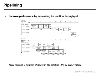
Pipelining • Performance optimization technique based on the overlap of the execution of multiple instructions deriving from a sequential execution flow. • Pipelining exploits the parallelism among instructions in a sequential instruction stream. • Basic idea: The execution of an instruction is divided into different phases (pipelines stages), requiring a fraction of the time necessary to complete the instruction. • The stages are connected one to the next to form the pipeline: instructions enter in the pipeline at one end, progress through the stages, and exit from the other end, as in an assembly line.
Pipelining • Advantage: technique transparent for the programmer. • Technique similar to a assembly line: a new car exits from the assembly line in the time necessary to complete one of the phases. • An assembly line does not reduce the time necessary to complete a car, but increases the number of cars produced simultaneously and the frequency to complete cars.
Pipelining • The time to advance the instruction of one stage in the pipeline corresponds to a clock cycle. • The pipeline stages must be synchronized: the duration of a clock cycle is defined by the time requested by the slower stage of the pipeline (i.e. 2 ns). • The goal is to balance the length of each pipeline stage • If the stages are perfectly balanced, the ideal speedup due to pipelining is equal to the number of pipeline stages.
Performance Improvement • Ideal case (asymptotically):If we consider the single-cycle unpipelined CPU1 with clock cycle of 8 ns and the pipelined CPU2 with 5 stages of 2 ns : • The latency (total execution time) of each instruction is worsened: from 8 ns to 10 ns • The throughput (number of instructions completed in the time unit) is improved of 4 times:(1 instruction completed each 8 ns) vs. (1 instruction completed each 2 ns)
Performance Improvement • Ideal case (asymptotically): If we consider the multi-cycle unpipelined CPU3 composed of 5 cycles of 2 ns and the pipelined CPU2 with 5 stages of 2 ns : • The latency (total execution time) of each instruction is not varied (10 ns) • The throughput (number of instructions completed in the time unit) is improved of 5 times: (1 instruction completed every 10 ns) vs. (1 instruction completed every 2 ns)
Visualizing Pipelining Reg Reg Reg Reg Reg Reg Reg Reg Ifetch Ifetch Ifetch Ifetch DMem DMem DMem DMem ALU ALU ALU ALU Cycle 1 Cycle 2 Cycle 3 Cycle 4 Cycle 5 Cycle 6 Cycle 7 Time (clock cycles) I n s t r. O r d e r
Note: Optimized Pipeline • Register File used in 2 stages: Read access during ID and write access during WB • What happens if read and write refer to the same register in the same clock cycle? • It is necessary to insert one stall • Optimized Pipeline: the RF read occurs in the second half of clock cycle and the RF write in the first half of clock cycle • What happens if read and write refer to the same register in the same clock cycle? • It is not necessary to insert one stall From now on, this is the Pipeline we are going to use
5 Steps of MIPS DatapathFigure A.3, Page A-9 MEM/WB ID/EX EX/MEM IF/ID Adder 4 Address ALU Instruction Fetch Execute Addr. Calc Memory Access Instr. Decode Reg. Fetch Write Back Next PC MUX Next SEQ PC Next SEQ PC Zero? RS1 Reg File MUX Memory RS2 Data Memory MUX MUX IR <= mem[PC]; PC <= PC + 4 Sign Extend WB Data Imm A <= Reg[IRrs]; B <= Reg[IRrt] RD RD RD rslt <= A opIRop B WB <= rslt • Data stationary control • local decode for each instruction phase / pipeline stage Reg[IRrd] <= WB 42