Download

1 / 17
210 likes | 419 Vues
HP Bead Probe Technology Evaluation. By TJ Choo and Rosa Reinosa Global Engineering Services – Palo Alto 09/15/09. Contents. Goals & Objectives Background Key Learnings Conclusions. Goals & Objectives. Evaluate bead probe manufacturability and its application to HP products

E N D
HP Bead Probe Technology Evaluation By TJ Choo and Rosa Reinosa Global Engineering Services – Palo Alto 09/15/09
Contents • Goals & Objectives • Background • Key Learnings • Conclusions
Goals & Objectives • Evaluate bead probe manufacturability and its application to HP products • Determine risks, challenges and ways to overcome them • Apply learnings on future product implementations
DOE Objectives Mfg Bead Probe Evaluation Assess performance and feasibility of new technology Characterize contact performance using various trace sizes, SRO sizes, stencil thickness, paste apertures and probe forces Life Tests Evaluation Characterize long term performance in an ICT or functional test environment Measure probe contact cycles before cleaning or replacement is needed
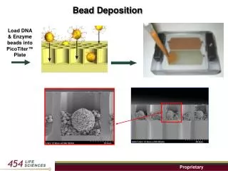
Background • Test Vehicle Description • 4 trace widths: 3, 4, 6 and 7 mils • SRO shape: Oval • SRO Width = Trace W + 6 mils to allow soldermask registration tolerance of +/- 3 mils • 5 SRO lengths were tested: 10, 15, 20, 25 and 30 mils • 10 mils and 30 mils SRO lengths were used as margin tests • Total beads per TV: 17,088 • Board Qty: Life Tests: 24 boards & Mfg Test: 18 boards • Process: OM338-PT with SSSR, DSSR, DSDR • Paste Stencil Design • Stencil thickness: 5 mils • Two stencil shapes: Diamond and Oval CLOSEUP
SRO Shape and Bead Formation • Solder beads can fail to form or attach to the Cu trace area • Trace width and SRO interact by determining the exposed Cu area in both length and width • SRO Design – SRO Registration Risks • Oval (per Agilent BP Handbook) • Solder mask registration tolerance reduces Cu bonding area • Rectangular (HP’s alternate approach) • Maintains a constant Cu bond area even when solder mask registration is off (within tolerance) Preferred SROL=20 mil SROW=WTRC+2xTol
SRO Shape • SRO Design – SRO Shape • Shape: Rectangular • SRO Length: 15~25 mils; 20 mils recommended for traces from 3~8 mils wide(length <15 mils increases bond risk –especially for trace widths < 5 mils) • SRO trace width plus 2x soldermask registration tolerance • e.g., for a 4 mil trace and soldermask registration tolerance of +/– 3 mils, use 10 mils minimum SRO width
Bond and Short Risks • Solder mask (SM) registration tolerance • Deficient SRO to Cu clearance leads to solder bond risk(next slide upper sample [1]) • Deficient trace spacing and/or SRO dam lead to shortrisk (next slide lower sample [2]) • Design using standard soldermask registration process tolerance • Avoid the costs and risks of using technology limits • Manage process tolerance through design guidelines
Trace Width and Spacing • Select Node Candidates for Bead Probe • Use bead probe only where there is no other way to test a node • Nodes impacted by signal integrity when placed on pads or vias • Nodes that are inaccessible due to high board density • Trace Width • Set PCB stackup so that the widest trace can be used • Trace-to-Trace Spacing • Must be managed properly to avoid bond and short risk issues due to solder mask (SM) registration tolerance • Follow guidelines for SRO to Cu clearance and minimum soldermask dam • Tightly coupled differential pairs require proper board layout design • Signal integrity not affected when spacing is properly managed • Trace lengths must be managed to avoid potential timing issues
Tightly Coupled Differential Pairs The delta among (a) trace without bead, (b) variable spacing differential paired impedance and (c) trace with bead are less than 1.0 [Ω] Z0 for all scenarios is less than 3% of theoretically calculated value This approach has been proven not to affect signal integrity
Paste Stencil and Silkscreen • Paste Stencil • Beads must have apertures that span the entire exposed Cu area on the trace to insure wetting and avoid unattached solder beads • Compute solder paste volume for bead heights of 4.5~7 mils, taking into account paste metal ratio (MR) by volume and transfer efficiency (TE) • Use 4.5 mil bead height for 3 mil traces • Increase bead height by 0.5 mils per 1.0 mil increase in trace width up to 6 mils max • Use elongated oval paste or obround apertures for better paste release • Minimum width: 9 mils • Cover entire length of SRO • Silk Screen Registration • Maintain proper clearance from any board silk screen markings to the exposed Cu areas for beads (SROs) • Maintain proper clearance from any silk screen (SS) board markup to SROs • Failure to do so may lead to markup encroaching on bead Cu areas and interfering with bead bonding • Specify no silkscreen encroaching allowed over solder bead Cu lands
Bead Height Risks Bead height is critical for reliability and contact Too high a bead is susceptible to damage by breaking off from the trace Too low a bead may lead to poor contact due to: Bead not rising sufficiently high above the solder mask to avoid mechanical interference Bead not rising sufficiently high above the flux residue, which may interfere when attempting to make electrical contact 13
Bead Orientation & Paste Aperture Considerations • Square paste stencil apertures • Can lead to improper bead heights due to their inherently lower Area Ratio • Lead to “dry spots” at the ends of beads due to the lower spread behavior of SAC lead-free solders • Oval and rectangular paste apertures may be able to overcome these difficulties of only using square apertures • However, orientation of beads may be a factor for oval and rectangular paste apertures with high L/W ratios • Hence, oval and rectangular paste stencil aperture dimensions should be kept as symmetrical as possible in the x and y directions; i.e., as close to round or square as possible • Make aperture L 4 to 6 mils over bead L and adjust aperture W as needed, keeping the Length/Width ratio as close as possible while avoiding the dry spots
Board and Fixture Design • Plan proper spacing and keepouts for solder beads. Account for spacing required for the probes • Stagger bead probes along traces to provide proper spacing without separating traces • For trace-to-trace spacing of less than 10 mils see how to implement bead probe tightly coupled differential pairs • Provide clearance of 75 mil minimum from edge of flat face probe and edge of component • Avoid contact obstruction from components, leads or other objects on board • Check with ICT fixture vendor for keepout guidelines around components and leads • Alternatively use the following minimum rule-of-thumb keepouts for objects up to 0.25” in height: • Board bottom: 75 mils (bead center to edge of component, lead or object) • Board top: 150 mils (bead center to edge of component, lead or object) • For higher than 0.25” objects: increase above keepouts 10 mils per 0.1” of added height (250 mils total max)
Process and ICT Risks • Process • Avoid any interaction of wave flux with bead. Flux residues from wave makes probe penetration harder • Paste • Select solder paste that is pin testable and is not so gummy that it will accumulate on probes • Probe Selection (Life Tests) • Use flat faced probes • Use 100 mil pitch where possible or QA 75 X-probe or equivalent for tighter spacing (36 mil Ø) • Avoid probe face Ø < 25 mils • When probes face Ø < 30 mils use a guided probe top plate • Try using the larger faced probes • Use 6.5 to 8.1 oz force probes for lead-free no-clean process
Conclusions • Bead probe technology is feasible and can be made to work with proper process control • Key control variables are solder mask registration and SRO shape • Trace width in combination with SRO length (most reliable is 20 mils) have the greatest impact on bead formation • Flux residue contamination is also a challenge for bead probe. Solder paste selection is critical. • Increasing probe force does not improve electrical contact