Download
1 / 28
280 likes | 451 Vues
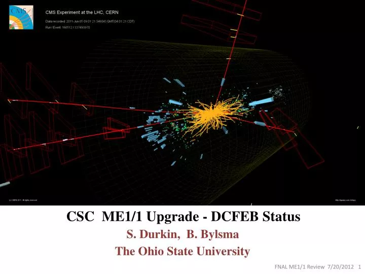
CSC ME1/1 Upgrade - DCFEB Status S. Durkin, B. Bylsma The Ohio State University. DCFEB R&D Prototype . ● Same size as old CFEB board ● Same input connections and 6 BUCKEYE amplifier-shaper ASICs ● 12 Texas Instruments ADS5281 ADC (8-channel, 12-bit, 50 MSPS, serial LVDS output)

E N D
CSC ME1/1 Upgrade - DCFEB Status S. Durkin, B. Bylsma The Ohio State University
DCFEB R&D Prototype ● Same size as old CFEB board ● Same input connections and 6 BUCKEYE amplifier-shaper ASICs ● 12 Texas Instruments ADS5281 ADC (8-channel, 12-bit, 50 MSPS, serial LVDS output) ● 4 options for preamp/ADC interface to evaluate ● 2 legacy skewclear connectors compatible with old TMB and DMB ● 3.2Gbps optical links to new TMB and new DMB ● Xilinx Virtex-6 XC6VLX130T-FFG1156 FPGA ● 20-layer PCB
R&D Prototype DCFEB Status A Dead timeless CFEB ● Two initial prototypes under tests since spring 2011 - bench tests at OSU - on ME2/1 chamber in B904 in place of old CFEB - trigger optical path (comparator hits) tested with new TMB (3.2Gbps) - DAQ optical path (digitized samples) tested with another DCFEB (3.2Gbps) ● It works 1:1 Replacement for Present CFEB ● All components Radiation Tested to HL LHC exposure ● Low level firmware and DCS software is mature
Buckeye 5-pole plus 1-pole 1-zero Fits View in Powerpoint Slide Show to See Movie of 16 channels Blue Data Black Fit adc counts t (nsec)
Fit Results by Coupling Type • Quad Diff, Single Diff, and DC coupling reproduce same shape to 1% • All Buckeye couplings work except AC so reject option • Gain is ~0.93 mV/fC. There is a small difference in pulse shape between DCFEB and CFEB pulses. The DCFEB peaks at 4/p0=103 nsec while the CFEB peaks at 106 nsec. There is an extra pole somewhere.
Linearity and Saturation Test • Inject amplifier channels with 18 linear steps in • voltage • Fit Buckeye Pulses to 5 pole shaper with 1-pole • 1-zero tail cancellations ADC(mV) Q inject (fC) Q (ADC counts) ADC Difference (mV) t (nsec) Q inject (fC)
Linearity and Saturation Test: Gain Gain is 0.95 mV/fC (same as old buckeye board)
Slewing, Capacitance Load Amplifier Slewing ~3 nsec Load Buckeye Input with Capacitance C (ADC Counts) 0 pF 1.5 100 pF 1.7 300 pF 2.2 500 pF 2.7 ADC (fC) C Qpeak(counts)tpeak(nsec) 0 pF 2671 101 100 pF 2600 102 300 pF 2432 108 500 pF 2264 117 t peak (nsec)
DCFEB Prototype Channel Noise DCFEB Pedestals – Typical Chip DCFEB and CFEB1 Noise RMS(ADC counts) ADC counts CFEB 1 DCFEB Channel Channel DCFEB Prototype Quieter than Old CFEB No SCA so noise reduces by 1.3 ADC counts in quadrature
DCFEB Radiation Testing ● Almost all DCFEB Components Tested before CFEB production ● Virtex 6 extensively radiation tested (see Jason Gilmore talk) Irradiation • Done at Crocker Nuclear Laboratory, U.C. Davis • June 14-15, 2012 • Proton Energy: 64 MeV • Chips irradiated to integrated dose of 30Krads • Corresponds to expected HL-LHC rates • SEU Testing on Flash ADC • Fixed patterns (alternating 0's and 1's) shifted at 20 MHz from FLASH ADC to Virtex6 FPGA • Firmware in Virtex 6 checked patterns for SEU upsets
DCFEB Radiation Testing (cont.) • SEU Testing Results • Firmware registered errors 12 times in total fluence of 2.3*1011 p/cm2 • 1 error clearly due to SEU in ADC • Unclear if other 11 errors were due to SEUs in ADC or the FPGA • In these cases, it was necessary to reprogram the Virtex 6 and restart the software before resuming • Therefore can set upper limit of 12 SEU/2.3*1011 p/cm2 SEU Flux • LHC neutron fluence is 6*1011 n/cm2 in 10 years • HL-LHC neutron fluence expected to be 5 times • = 5.4 SEU/hr
DCFEB Radiation Testing (cont.) • Radiation Damage Test of Flash ADCs and Differential Amplifiers • 12 ADCs on board, 2 were exposed (1 top, 1 bottom) • 8 op amps, 4 were exposed (2 top, 2 bottom) • Calibration pulses taken before irradiation as a baseline. Data read out from all 12 ADCs. • Stopped irradiation at regular intervals to redo calibration pulses. • Calibration pulses taken after final dosage of 30Krads. • No observable degradation of either chip was measurable.
DCFEB Radiation Testing (cont.) • Typical Pulse vs. Time (Temperature Corrected) Before and After 30 Krad Irradiation
DCFEB Radiation Testing (cont.) Temperature Corrected Before and After Difference (ADC Counts) 30 Krad No Radiation
DCFEB Radiation Testing (cont.) Results for ADC and Op Amp • No measurable difference in op amp after 30 Krads • Small DC shift in ADC, at most 5 ADC counts(noise on chamber ~4 ADC counts) after 30 Krads Conclusions • 5 devices tested • Op amp: TI THS4524IDB • ADC: TI ADS5281IPFP • Buffer: SN74LVC244APW • PROM: XCF128XFT64C • JTAG Mux: SN74LVC157ARGY • All survived 30 Krads TID • ADC SEU flux is 1.5*10-3 SEU/s for system ALL DCFEB COMPONENTS ARE RADIATION HARD
Firmware/Software Development ● A Core Part of Modern Electronics is Firmware/Software - More than 6 man-months work - ~8000 lines of c-code FPGA Firmware DAQ - pipeline (done) - trigger primitive to TMB (done) - optical data path to DMB (done) - JTAG and trigger communications copper (done) FF_EMU path interface (not implimented/untested) - tripple-voting (not implimented) - circular buffer instead of FIFO for data path (not implimented) - External DAC and ADC control (not implimented) - autoloading constants from EPROM (not implimented)
Firmware/Software Development (cont.) FGPA Timing Constants Firmware constants have to be writeable from JTAG and autoloaded from EPROM - pipleline length (done) - fine daq timing (clock phase adjustment)(not implimented in software/firmware) - fine trigger primitive timing (clock phase adjustment)(not implimented in software/firmware) FPGA Communications Software - load Virtex 6 thru JTAG (done) - readback and verify Virtex 6 thru JTAG (done) - readbackusrcode and id (done) - read/write Virtex 6 status registers (done) - temperatures (not implimented) - voltages (not implimented) - Comp. DAC/Cal DAC/Ext. ADC control migration from DMB to DCFEB (not implimented)
Firmware/Software Development (cont.) FPGA SEU Scrubbing Software/Firmware - firmware: Virtex 6 auto scrubbing (not implimented) - sofware: selective read and write of Virtex 6 blocks for SEU correction (done) EPROM/FPGA communications Software - loading Virtex 6 firmware (done) - readback and verify Virtex 6 firmware (done) - loading constants in upper EPROM memory (done) - autoload constants from EPROM memory (not implimented) preproduction DCFEBs will be ready immediately to start full system tests
Pre-Production DCFEB Boards ● Production prototype: - remove excessive R&D options - few minor changes (add DAC for calibration references and ADC for monitoring, replace voltage regulator with rad hard Micrel part) ● Layout finish June 16, 2012 - delay 2.5 months: CMS CSC Readout Crisis: DDU/DCC firmware rework during 2011 shutdown (Bylsma, Durkin, Gilmore) ● 10 PC Boards Compunetics Monroeville, PA - delayed 3 weeks: ran out of materials ● 10 boards Stuffed Compunetics Reynoldsburg, OH ● 10 boards will be debugged early next week, 7 will be sent to CERN - 3 will be distributed to groups writing firmware/software
ME1/1 Electronics Integration ● Integration has already started at Bldg 904 CERN - software communications between DMB and prototype DCFEB accomplished - ~8000 lines of DCFEB code committed to TriDAS/emu/emuDCScvs repository ● Hope to have ODMB at CERN early August - by end of september must prove trigger, data, and communication paths work - time in the system to trigger and readin cosmic rays and high rate triggers Problem: FF-EMU ASIC prototype does not work. Needed for signal communications If EPROM and Virtex6 simultaneously lose firmware. (see Guido’s talk)
Signal Connections to DCFEBs • Present system: • Trigger, DAQ, clock and control signals transmitted over copper Skewclear cables. • DAQ signal data rate is 280Mbps and up to 15m for some ME1/1 chambers. • Length and rate are on the edge of reliability. Have had some connection issues. • DCFEB system (all optical): • Replace all copper connections with fiber optics. • Requires FF-EMU ASIC and uses FFLYNX protocol to encode/decode trigger, • timing. and control signals. • DCFEB system (backup option 1): • Comparator signals to TMB and DAQ signals to ODMB transmitted over fibers. • Trigger, timing and control signals transmitted over copper to DCFEBs. • FourSkewclear cables to patch panel (PP), seven cables to PP-to-DCFEBs • Patch panel is a passive PCB for cable interconnections. • LVDS signals routed through impedance controlled board. • DCFEB system (backup option 2): • Same as backup option 1 except: • Two Skewclear cables to patch panel (PP), seven cables to PP-to-DCFEBs • Patch panel is a active PCB with LVDS repeaters for cable interconnections.
ME1/1 DCFEB/ODMB/TMB Connections All optical Solution TRG TX (comp. data) DAQ TX (ADC data) CTRL TX (FFEMU uplink) CTRL RX (FFEMU downlink) CLK320 (main clock) ALTCLK40 (alternate clock) DCFEB1 Optical Patch Panel TRG TX (comp. data) DAQ TX (ADC data) CTRL TX (FFEMU uplink) CTRL RX (FFEMU downlink) CLK320 (main clock) ALTCLK40 (alternate clock) Peripheral Crate DCFEB2 TMB TRG RX TRG TX (comp. data) DAQ TX (ADC data) CTRL TX (FFEMU uplink) CTRL RX (FFEMU downlink) CLK320 (main clock) ALTCLK40 (alternate clock) DCFEB3 12/12 50 7/12 7/12 7/12 9/12 12 12 50 12 12 12 Trigger Up Fan outs on chamber (equal lengths for all chambers) TRG TX (comp. data) DAQ TX (ADC data) CTRL TX (FFEMU uplink) CTRL RX (FFEMU downlink) CLK320 (main clock) ALTCLK40 (alternate clock) ODMB DAQ RX CTRL RX CLK/CTRL TX A CLK/CTRL TX B LVMB DCFEB4 DAQ Up Control Up TRG TX (comp. data) DAQ TX (ADC data) CTRL TX (FFEMU uplink) CTRL RX (FFEMU downlink) CLK320 (main clock) ALTCLK40 (alternate clock) Clk/cntrl Down A DCFEB5 Clk/cntrl Down B LVMB (copper) TRG TX (comp. data) DAQ TX (ADC data) CTRL TX (FFEMU uplink) CTRL RX (FFEMU downlink) CLK320 (main clock) ALTCLK40 (alternate clock) DCFEB6 Existing Skewclear Multi-fiber bundles Equal lengths within chamber groups Can be various lengths chamber-to-chamber TRG TX (comp. data) DAQ TX (ADC data) CTRL TX (FFEMU uplink) CTRL RX (FFEMU downlink) CLK320 (main clock) ALTCLK40 (alternate clock) LVMB DCFEB7
ME1/1 DCFEB/ODMB/TMB Connections With Copper Backup Solution Option 1 (Passive interconnects) TRG TX (comp. data) DAQ TX (ADC data) 50 pin copper SCSI connector DCFEB1 Mixed Optical/Copper Patch Panel Peripheral Crate TRG TX (comp. data) DAQ TX (ADC data) 50 pin copper SCSI connector DCFEB2 TMB TRG RX TRG TX (comp. data) DAQ TX (ADC data) 50 pin copper SCSI connector DCFEB3 50 Min25 7/12 7/12 50 50 50 50 12 12 50 Trigger Up Optical TRG TX (comp. data) DAQ TX (ADC data) 50 pin copper SCSI connector DCFEB4 ODMB DAQ RX Trg/CtrlA Trg/CtrlB Trg/CtrlC Trg/CtrlD LVMB DAQ Up Optical TRG TX (comp. data) DAQ TX (ADC data) 50 pin copper SCSI connector PCB Passive Interconnects TTC1 DCFEB5 TTC2 TTC3 TTC4 TTC5 TRG TX (comp. data) DAQ TX (ADC data) 50 pin copper SCSI connector TTC6 DCFEB6 TTC7 LVMB TRG TX (comp. data) DAQ TX (ADC data) 50 pin copper SCSI connector DCFEB7 Existing Skewclear cables from PC to PP Utilizes five out of ten available cables. PCB with SCSI connectors interconnected with 100 ohm differential signal pairs. No power required. On-chamber cables. (Skewclear not required). LVMB
ME1/1 DCFEB/ODMB/TMB Connections With Copper Backup Solution Option 2 (Active LVDS Repeaters) TRG TX (comp. data) DAQ TX (ADC data) 50 pin copper SCSI connector DCFEB1 Mixed Optical/Copper Patch Panel Peripheral Crate TRG TX (comp. data) DAQ TX (ADC data) 50 pin copper SCSI connector DCFEB2 TMB TRG RX TRG TX (comp. data) DAQ TX (ADC data) 50 pin copper SCSI connector DCFEB3 50 Min25 7/12 7/12 50 50 12 12 50 Trigger Up Optical TRG TX (comp. data) DAQ TX (ADC data) 50 pin copper SCSI connector DCFEB4 ODMB DAQ RX Trg/CtrlA Trg/CtrlB LVMB DAQ Up Optical TRG TX (comp. data) DAQ TX (ADC data) 50 pin copper SCSI connector PCB Active LVDS Repeaters TTC1 DCFEB5 TTC2 TTC3 TTC4 TTC5 TRG TX (comp. data) DAQ TX (ADC data) 50 pin copper SCSI connector TTC6 DCFEB6 TTC7 LVMB TRG TX (comp. data) DAQ TX (ADC data) 50 pin copper SCSI connector DCFEB7 Existing Skewclear cables from PC to PP Utilizes three of ten cables. PCB with SCSI connectors and active LVDS repeaters. Power supplied by ODMB. On-chamber cables. Skewclear not required. LVMB
Status of Copper Backup Solution • Dubna group working on mock-ups to study integration issues at the patch panel. • Space constraints suggest two PCB boards may be necessary to accommodate the connectors and cable bending radius.
Production of 656 DCFEBs ● Production Review Mid-October - changed due to LHC Schedule 3 month slip ● Procure Parts - large order so will go out for bids - electronics houses don’t typically have 600 of expensive parts (6-8 week delays possible) ● PC Board Production: Compunetics - sole source (competitive bid?), $50/board typical quote difference) - will specify a few boards, a delay, then full production ● Stuffing: DynaLab - competitive, Dynalab seems to be a lot cheaper than other companies - will specify a few boards, a delay, then full production Expect Delays in Board Construction Schedule out of our hands…
Production of 656 DCFEBs (cont.) ● DCFEBs will be tested and repaired at OSU - OSU technician will help - software already written - software take ~3 minutes/board - expect ~10 boards a day - serial number on board and transferred to prom will identify board ● Boards will be shipped as they pass tests - in the past we have shipped in lots of 20 boards - burn-in will be done at CERN - chamber mounting and integration at CERN
DCFEB Conclusions R&D Prototype DCFEB ● It works 1:1 Replacement for Present CFEB ● All components Radiation Tested to HL LHC exposure ● Low level firmware and DCS software is mature Pre-Production Prototype ● 10 boards delivered today ● 7 Boards to be shipped to CERN next week ● System Integration underway at CERN ● Copper Cable backup under study Production 656 DCFEBs ● No problems anticipated