Download
1 / 20
200 likes | 366 Vues
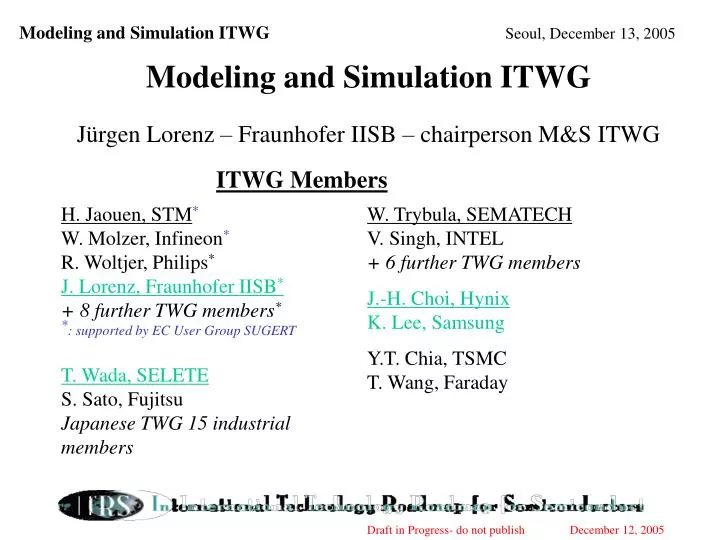
Modeling and Simulation ITWG Jürgen Lorenz – Fraunhofer IISB – chairperson M&S ITWG. ITWG Members. H. Jaouen, STM * W. Molzer, Infineon * R. Woltjer, Philips * J. Lorenz, Fraunhofer IISB * + 8 further TWG members * * : supported by EC User Group SUGERT T. Wada, SELETE S. Sato, Fujitsu

E N D
Modeling and Simulation ITWG Jürgen Lorenz – Fraunhofer IISB – chairperson M&S ITWG ITWG Members H. Jaouen, STM* W. Molzer, Infineon* R. Woltjer, Philips* J. Lorenz, Fraunhofer IISB* + 8 further TWG members* *: supported by EC User Group SUGERT T. Wada, SELETE S. Sato, Fujitsu Japanese TWG 15 industrial members W. Trybula, SEMATECH V. Singh, INTEL + 6 further TWG members J.-H. Choi, Hynix K. Lee, Samsung Y.T. Chia, TSMC T. Wang, Faraday
2005 Modeling&Simulation SCOPE & SCALES • Equipment related • Equipment/Feature scale Modeling • Lithography Modeling • Feature scale • Front End Process Modeling • Device Modeling • Interconnects and • Integrated Passives Modeling • IC-scale • Circuit ElementsModeling • Package Simulation • Modeling Overall Goal • Support technology • development and optimization • Reduce development times • and costs • • Materials Modeling • • Numerical Methods • DFM / DFY
Key Messages (I) • Mission of Modeling and Simulation as cross-cut topic: • Support areas covered by other (especially focus) ITWGs • In-depth analysis of M&S needs of other ITWGs performed, based on • documents + inter-ITWG discussions • Modeling and simulation provides an ‘embodiment of knowledge and understanding’. It is a tool for technology/device development and optimization and also for training/education • Technology modeling and simulation is one of a few enabling methodologies that can accelerate development times and reduce development costs: Assessment up to 35% already in 2003 • (when simulation is used efficiently) • important not only in years of difficult economic conditions
Key Messages (II) • Art of modeling: • - Combine dedicated experiments & theory to extract physical mechanisms • & parameters • - Find appropriate trade-off between detailed physical simulation (CPU and • memory costly) and simplified but physically appropriate approaches • Accurate experimental characterization methods are essential • Reliable experimental reference data required on all levels – profiles, electrical data, ….. – must partly be provided e.g. by device makers! • Further growing importance of atomistic/materials/hierarchical/multilevel simulation - appropriate treatment of nanostructures • Invitation for extended participation esp. from Korea and Taiwan • - Korean TWG now extended
Crosscuts between M&S and other ITWGs • Detailed analysis of other ITRS chapters + discussions with other ITWGs as basis for 2003 M&S challenges and requirements tables, and text • This process continued in 2004 - emphasis on tables – and in 2005 • Crosscuts with focal ITWGs and other cross-cut ITWG being described in detail • Links with ALL other ITWGs. Some examples: • Design: Influence of process fluctuations, intrinsic statistics, noise, • reliability, ... on design • Test: Extension of interconnect simulation towards simulation • of test equipment. Assess if defects detected are critical. • PIDS: Long list including modeling of new processes, materials and device architectures, atomistic/quantum mechanical simulation, • fluctuations and variations, coupled device/circuit/system • simulation
Crosscuts between M&S and other ITWGs (cont.) • Some examples (cont.): • ERD: First-principle simulation, esp. including other state variables • than charge • RF/AMS: Include III/V compounds. Accurate and fast 3D EM, RF and • thermal simulation • FEP: Long list including modeling of material issues, impact of • interfaces, new device architectures, ultra-shallow junctions and • defect engineering, assessment of process variants Lithography: Push limits of optical lithography by optimization of options; assessment of Next Generation Lithography based on predictive physical models. Describe immersion lithography, LER, LWR. Support Design for Manufacturing • Interconnects: Large range of M&S support needed, from prediction of material • properties (e.g. resistivity of narrow Cu lines) to impact of • non-idealized interconnects on IC layout
Crosscuts between M&S and other ITWGs (cont.) • Some examples (cont.): • Factory Int.: Support shrink of technology implemented in fab line by • equipment/process/device/circuit simulation. • Assess impact of process variations on yield • Assembly and Packaging: • Co-design issues: Chip and package, mechanical/electrical/ • thermal simulation. Design and process tolerances esp.for BEOL • ESH: Bi-directional link w.r.t characterization and models for gas • composition and chemical reactions. Support reduction of • material consumption • Yield Enhancement: • Simulation influence of defects and of process fluctuations on • devices/ICs/yield. Support development of APC models • Metrology: M&S needs advanced metrology for development/assessment of • physical models. Physical modeling to support metrology e.g. • w.r.t. linking measured spectra to gas composition, interpretation • of measured data, extension of measurements from 2D to 3D
Basic Approach and Focus of 2005 Work • Detailed cross-cuts worked out in 2003 – regularly updated together with other ITWGs • Tables strongly revised in 2004 – in 2005 mainly adaptations in timing and some updates • Rewrite of text, based on 2004/2005 changes of crosscuts and tables, and state-of-the-art • Involve subchapter editing teams which should consist of representatives from each region (achieved: 3 to 5 region involved) • Main 2005 change in chapter structure: • Add new subchapter on TCAD for Design, Manufacturing and Yield: Development & use of simulation to assess impact of process variations on device & circuit performance, manufacturing, yield, …
2005 Short-term Difficult Challenges High-Frequency Device and Circuit Modeling for 5-100 Ghz Applications • Needs • Efficient extraction and simulation of full-chip interconnect delay and power consumption • Accurate and yet efficient 3D interconnect models, especially for transmission lines and S-parameters • Extension of physical device models to III/V materials • High-frequency circuit models including non-quasi-static effects, substrate noise, 1/f noise and parasitic coupling • Parameter extraction assisted by numerical electrical simulation instead of RF measurement • Scalable active and passive component models for circuit simulation • Co-design between interconnects and packaging (From Philips)
2005 Short-Term Difficult Challenges Front-End Process Modeling for Nanometer Structures Needs • Diffusion/activation/damage/stress models and parameters incl. SPER and low thermal budget processes in Si-based substrate, e.g. Si, SiGe:C, Ge, SOI, epilayers and ultra-thin body devices • Modeling of epitaxially grown layers: Shape, morphology, stress • Characterization tools/methodologies for these ultra-shallow geometries/ junctions and low dopant levels • Modeling hierarchy from atomistic to continuum for dopants and defects in bulk and at interfaces • Front-end processing impact on reliability Source: P. Pichler et al., Proc. IEDM 2004
2005 Short-Term Difficult Challenges Integrated Modeling of Equipment, Materials, Feature Scale Processes and Influences on Devices Needs • Fundamental physical data ( e.g. rate constants, cross sections, surface chemistry for ULK, photoresists and high-k metal gate); reaction mechanisms and simplified but physical models for complex chemistry and plasma reaction • Linked equipment/feature scale models (including high-k metal gate integration, damage prediction) • CMP, etch, electrochemical polishing (ECP) (full wafer and chip level, pattern dependent effects) • • MOCVD, PECVD and ALD, electroplating and electroless deposition modeling • • Multi-generation equipment/wafer models Simulated across-wafer variation of feature profile for a sputter-deposited barrier. (From Fraunhofer IISB)
2005 Short-Term Difficult Challenges Lithography Simulation including NGL Needs • Optical simulation of resolution enhancement techniques including mask optimization (OPC,PSM) • Predictive resist models (e.g. mesoscale models) incl. line-edge roughness, etch resistance, adhesion, and mechanical stability • Methods to easily calibrate resist model kinetic and transport parameters • Models that bridge requirements of OPC (speed) and process development (predictive) • Experimental verification and simulation of ultra-high NA vector models, including polarization effects from the mask and the imaging system • Models and experimental verification of non-optical immersion lithography effects (e.g. topography and change of refractive index distribution) • Multi-generation lithography system models • Simulation of defect influences / defect printing • Modeling lifetime effects of equipment and masks Example: Footing effect in vicinity of shadowed region at bottom of poly-Si line Top-down wafer SEM (from T. Sato, Toshiba) 3D simulation (from A. Erdmann, FhG-IISB)
2005 Short-Term Difficult Challenges Ultimate Nanoscale CMOS Simulation Capability • Needs • • Methods, models and algorithms that • contribute to prediction of CMOS limits • • General, accurate and computationally • efficient quantum based simulators • • Models and analysis to enable design • and evaluation of devices and architec- • tures beyond traditional planar CMOS • • Gate stack models for ultra-thin • dielectrics • • Models for device impact of statistical • fluctuations in structures and dopant • distributions • Material models for stress engineering. • Physical models for stress induced • device performance classical quantum drain source courtesy Infineon / TU Munich courtesy Infineon / TU Munich Quantum-mechanical vs. classical carrier densitiy in double-gate transistor
2005 Short-Term Difficult Challenges Thermal-Mechanical-Electrical Modeling for Interconnects and Packaging • Needs • • Model thermal-mechanical, thermo- • dynamic and electronic properties of • low-k, high-k and conductors for • efficient in-chip package layout and • power management, and the impact • of processing on these properties • especially for interfaces and films • under 1 micron • • Model reliability of packages and • interconnects, e.g. stress voiding, • electromigration, piezoelectric • effects; textures, fracture, adhesion • Models for electron transport in ultra • fine patterned conductors courtesy TU Vienna / IST project MULSIC Temperature distribution in an interconnect structure
Requirement Tables: 2005 Changes • General: • Items adapted to 2 years passed since 2003 ITRS & changes in requirements/ technical progress • 2003 and 2004 information checked – partly requirements met, partly they influence 2005 etc. • Table continues to contain some items in “zebra” colour - according to ITRS guidelines: • “Limitations of available solutions will not delay the start of production. In some cases, work-arounds will be initially employed. Subsequent improvement is expected to close any gaps for production performance in areas such as process control, yield, and productivity.“ • This means for simulation: It can be used, but with more calibration, larger CPU time/memory, less generality then in the end required ...
Requirement Tables: 2005 Changes • Main changes in line headers: • New structure for “Numerical device modeling”: no more separation between “Classical CMOS” and “Non-classical CMOS”, but now between “Transport modeling” and “Additional requirements for non-classical CMOS” • In Numerical Analysis, new line for “Meshing” • Changes in line items • Several details changed in content and timing
More details given in tables & ITRS text • Thank you