Download
1 / 10
100 likes | 109 Vues
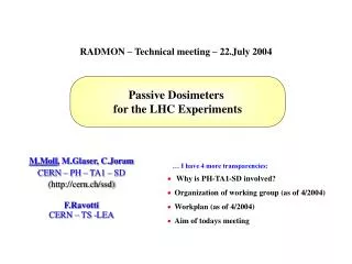
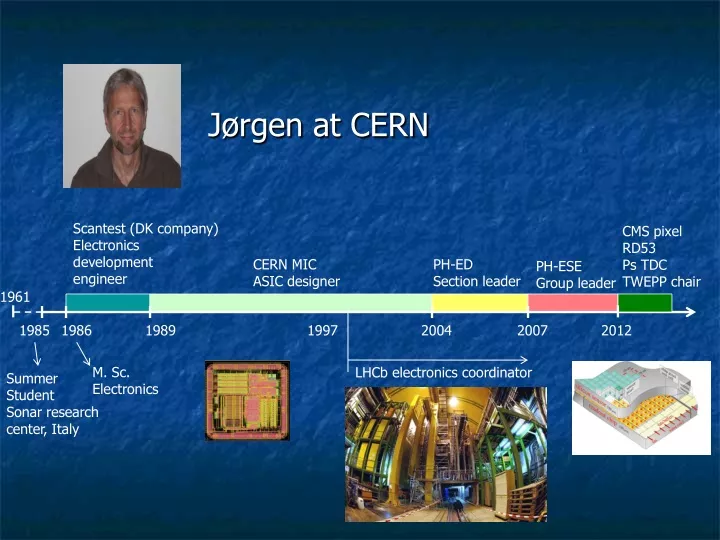
Scantest (DK company) Electronics development engineer. CMS pixel RD53 Ps TDC TWEPP chair. J ø rgen at CERN. CERN MIC ASIC designer. PH-ED Section leader. PH-ESE Group leader. 1961. 1985. 1986. 1989. 1997. 2004. 2007. 2012. M. Sc. Electronics.

E N D
Scantest (DK company) Electronics development engineer CMS pixel RD53 Ps TDC TWEPP chair Jørgen at CERN CERN MIC ASIC designer PH-ED Section leader PH-ESE Group leader 1961 1985 1986 1989 1997 2004 2007 2012 M. Sc. Electronics LHCb electronics coordinator Summer Student Sonar research center, Italy
Micro electronics at CERN 89-04 • Design of a large variety of ASIC’s in different technologies used in many experiments world wide. • Fastbus slave interface chip: ALEPH , NOMAD and NA48. • Architectural/simulation study of packet switching DAQ system • Time to digital converters: Drift based detectors and TOF • 16 channel TDC for NA48 • 32 channel general purpose TDC used by multiple experiments (at CERN and outside CERN) and commercial module (CAEN) • 32 channel 800ps TDC architecture for ATLAS MDT-> Implementation at KEK • Novel Pico-second resolution TDC’s and timing generators (with students) • 32 channel 800ps/200ps/100ps/25ps TDC with highly flexible data driven buffering/triggering and readout architecture. • CMSmuon detector • ALICE TOF • ~20 different experiments world wide • Commercial modules from 3 companies • 50k chips produced • Digital architecture and first implementation of Timing and Trigger Control (TTC) ASIC for LHC experiments. • IC tester and CAE design tools. • CMOS Technologies: 1.2 – 0,25 um • Gate array, Standard cell and Full custom level HPTDC HPTDC in ALICE TOF HPTDC in CMS muon
LHCb elec. coordination 97 - 07 Architecture • Organization and Coordination of electronics in LHCb • Defined, simulated and specified front-end electronics architecture. • Defined interfaces to trigger, DAQ and control systems. • Defined and enforced radiation hardness policy of electronics systems • EMC, Equipment safety, Web pages, Power supplies, Cabling, etc. • Organize electronics community in LHCb • Chaired electronics meetings in LHCb weeks • Organized regular electronics workshops • Indentify and enforced common solutions • Off detector/DAQ interface module, Control interfaces, Optical links, Power supplies, front-end chips, , • Review and verify electronics systems and designs: Chairing ~50 reviews • Architecture, Design, radiation tol., Production, system interfaces, EMC. • Define and manage general electronics infrastructure: Power distribution, racks, crates, cabling, detector safety system Radiation Services, Installation, Commissioning
PH-ESE group leader 2007 - 2011 • Merging 5 electronics groups into one global electronics support group servicing and driving R&D for CERN experiments. • Improved synergy/efficiencyto handle staff retirements 65 -> 50 • Support to experiments, services to HEP community, develop technologies needed for future experiments and upgrades, Coordinate HEP electronics, Organize/Participate in specific experiment projects , , • Define and implement new group structure • Micro electronics: Rad hard technologies and HEP ASIC’s • Front-end: On-detector electronics (rad hard, compact, detector interface, cooling, ,) • Back-end: Off-detector electronics (DAQ , trigger, links, power, pool, ) • Relocation of group into refurbished building • Global project management structure and interface to experiments • Electronics steering committee • ESE Group leader, PH management and management of experiments (Tech.+ Elec. Coord.) • Electronics coordination board • ESE Group leader and experiment representatives (Elec. Coord.) • Regular update on results/problems • Central forum for global electronics issues across experiments • Minimize duplication across experiments
PH-ESE ICs • Assuring vital services to community: • Electronics pool (~750 instruments, 5000 movements per year) • Low voltage power supplies and crates support/repair (6000 in experiments) • Power distribution and racks • IC technologies and associated design tools (complicated and expensive) • Radiation qualification, libraries, tools, MPW runs, frame contracts, export restrictions , , , • Launching vital common R&D (WP) • Rad hard IC technologies and required design tools (130nm + 65nm) • Rad hard optical link (GBT ASICs and opto modules) • Rad hard and magnetic field tolerant power conversion: On-detector DC/DC • High density interconnect (bump bonding and TSV) • Project specific R&D • NA62 GTK, pixel systems, strip systems, New TTC, , , • Technology transfer: Medipix/timepix/dosepix, TDC, • Exchange of experience between internal experts and external groups (collaborating institutes in experiments) • Bi-weekly electronics seminars • Well working group with a group “culture”covering all vital technologies and expertise needed. Modules Crates, Power supplies Systems, Experiments
Pixels detectors and chips 2012- Every 25nsum precision • CMS phase 2 pixel electronics coordination • To be installed in 2025 • Unpresented challenges on pixel size (50x50um2), hit rates (3GHz/cm2), radiation tolerance (1 Grad , 10.000 higher than space/mil), chip complexity (mixed signal chip with 1 billion transistors), etc. • Global system: • Definition of requirements, architecture and project organization • Pixel ASIC -> RD53 • Define requirements and architecture appropriate for >3GHz/cm2 hit rates Project/architecture definition and organization of involved groups • RD53 collaboration: ATLAS and CMS phase 2 pixel chip • Initiated (in 2012) RD53 collaboration to make extremely challenging next generation pixel detector ASICs for ATLAS and CMS • Urgent to get work started as pixel ASIC critical and looong development time • Unprecedented requirements: Small pixels, 3GHz/cm2, 1Grad, Readout rates, • ~1 Billion transistors in 65nm CMOS technology • RD53 co-spokesperson • Formation of collaboration, LHCC proposal –> Acceptance, Collaboration framework/organization • 4 ( plus 3) year R&D program to get to large high rate pixel ASIC • RD53A demonstrator chip submitted last year, final chips in 2019 • 22 Institutes, ~150 collaborators • LHCC status report: https://indico.cern.ch/event/726320/contributions/3005309/attachments/1658484/2656006/LHCC_status_report_2018_open.pdf Hybrid pixel RD53 demonstrator chip ATLAS Pixel Detector
Other activities • Radiation effects consultancy to the LHC • Underestimated radiation effects (single event upsets very close to compromise running the LHC) • Teaching and giving courses • Electronics for HEP detectors (summer student lectures) • Radiation effects • PicoTDC: High resolution detectors for future experiments • 64 channel 1ps time resolution ASIC in 65nm CMOS technology • Chip submission end of next month • TWEPP workshop chairman: 2014 – 2016 • Yearly workshop on electronics for high energy physics, ~200 participants • CERN management liaison for Denmark • Attract more Danish students to CERN • CERN student programs: • Dedicated trainee program for Danish master/bachelor level students: And not forgetting other activities • Winter: Downhill skiing, snowboard, cross country • Summer: Mountain walking, mountain biking
Summary • CERN is a great place to work • Lots of hard working and very motivated people • Lots of unique technical challenges • Unique international environment with people from all possible places/cultures • Geneva area is a nice place to live, just next to the Jura mountains and the Alps • Bringing a whole family here can be a unique opportunity with some challenges • Language • Kids and school (extremely international environment) • Work and integration of spouses
Background – Before CERN • 1985: Summer student at SACLANT research centre (NATO sonar research centre in La Spezia, Italy) • Development of DSP based linear sonar array calibration system based. Used to calibrate linear sonar arrays of institute. • 1986 : M. Sc. in electronics engineering • Digital signal processing • Micro processor design • IC design and technologies • Sonar and transducers (parametric array transducer) • 1986 – 1989: Electronics development engineer • Startup: 4-15 employees (spin-off from larger electronics company) • Commercialize IC test system developed in Danish research institute as part of EU project • Develop second generation system based on ASIC’s, Bit-slice processor and FPGA’s