Download
1 / 35
350 likes | 629 Vues
The work of GEM foil at CIAE. Li Ye, Xiaomei Li Science and Technology on Nuclear Data Laboratory China Institute of Atomic Energy 2011.08 weihai. outline. Patr 1: Motivation Part 2: The structure of GEM foil Part 3: Gem foil researches at CIAE

E N D
The work of GEM foil at CIAE Li Ye, Xiaomei Li Science and Technology on Nuclear Data Laboratory China Institute of Atomic Energy 2011.08 weihai
outline Patr 1: Motivation Part 2: The structure of GEM foil Part 3:Gem foil researches at CIAE Part 4: THGEM detector and test at IHEP Part 5: Next step
JLab 12GeV Upgrade Add 5 cryomodules 20 cryomodules Add 5 cryomodules 20 cryomodules New Hall Enhanced capabilities in existing Halls Add arc
SoLID spectrometer Transversity PVDIS longitudinal
CIAE,USTC,TSinghua,Peking,HUST,Shandong,Lanzhou,Huangshan,and so on
GEM (Gas Electron Multiplier) Structure • Avalanche Gaseous Detector • Core part: GEM Foil • Sealed by the window and the substrate to form a pressure-tight gaseous chamber Ar+CO2 Structure of detector with single GEM foil
GEM (Gas Electron Multiplier) Structure Ar+CO2 Structure of detector with triple GEM foils
GEM Foil Structure A sandwich structure 5-10μm copper foils on the surfaces of Kapton foils
GEM Foil Structure • A dipole field will form when a voltage is applied on the two sides of the foil, gathering the field lines between the drift electrode and read-out electrode into holes. • Avalanche happens in holes Field shape of a GEM foil Kapton foils have excellent mechanical, physical and chemical properties. They will not melt, burn, and they are flexible.
Process Flow Diagram of GEM Manufacture 1. Copper-plating on the two sides of Kapton foils. a Clad the 5-10μm copper foils on the surfaces of Kapton foils by hot-pressing. bMake 5-10μm copper foils on the surfaces of Kapton foils by vacuum deposition technique. 2.Photoresist coating. Pull the Kapton foil out of 303 negative photoresist, the thickness can be controlled by the pulling-out speed. 3.Lithography The patterns on the mask can be transferred to the photoresist layer, then wash it with developing solution. 4.Copper foil etching Washing the foil with 30% iron trichloride(FeCl3)solution, then the pattern on the photoresist layer can be transferred to the copper foil layer, the depth of etching can be controlled by controlling the etching time. 5. Kapton foil etching The most important step of the whole process flow diagram. processes
From Foils to Detectors GEM foil is flexible, it must be fixed by a frame, then it can be mounted on detectors. Processes of Fixation Fix by a fiberglass substrate Dry in 40°C circumstances Epoxy Dry and solidify A standard GEM foil
Read out Electrodes collecting avalanche electrons have crucial effects on spatial resolution, time resolution and detection efficiency. Principle of Read Out Parallel Strips and Pads Array Thin Film Transistor, TFT. CMOS. CCD.
Agreement with CERN Prof. Xiaomei LI has visited CERN PCB factory and GEM group in Feb. 2011 . We got two GEM foil samples and two mask plates from CERN. CERN PCB factory has agreedthat they would transfer the GEM foil production technology to CIAE for free for the research of high energy physics. Now we are doing the paper work.
GEM Foil from CERN 10cm*10cm GEM foil sample
GEM Mask Plate from CERN 10cm*10cm mask plate
GEM Foil Researches at CIAE 1. Kapton foil covered with copper has got from the manufacturer in china. 2. Photoresist coating and masking Cooperate with the factory, we can make 70μm diameter 5cm* 5cm mask plate 3. Copper etching ---some problems. It will be solved after getting the technology transfer from CERN. 4. Kapton etching CIAE has over 20 years nuclear pore foil production and kapton etching experience. 5. Clean room for GEMconstruction
Mask PlateMade in China 5cm*5cm mask plate
Nuclear Pore Foil Production at CIAE HI-13 accelerator particles are accelerated by HI-13 then pass through the kapton foil,kapton etching,20um,control the hole size by etching time
Cleanroom our 1K level cleanroom for etching,framing,cleaning and
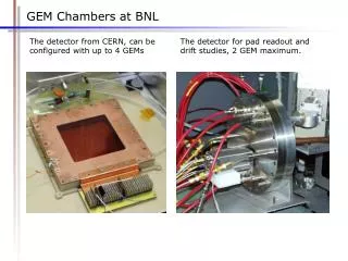
Introduction of Thick-GEM (THGEM) detector A. Breskin, M. Cortesi, R. Alon, J. Miyamoto & R. Chechik Weizmann institute of science, Rehovot, Israel radiation e-s EDrift EHole ETran EHole EInd Readout anode
Difference Between GEM and THGEM Foils GEM TH-GEM • Typical parameters: • 50mm Kapton • metal coated • Ø70mm holes • 100-200mm pitch Manufactured by standard PCB techniques of precise drilling in G-10 (and other materials) and Cu etching.
Some Results of THGEM from Breskin VHOLE [Volt] single electrons Single THGEM Gain 104-105 Double THGEMs gain 106-107 THGEM - Gain vs rim size Double-THGEM 6 keV x-rays 104 pitch = 1 mm; diameter = 0.5 mm; rim=40; 60; 80; 100; 120 mm Recent Advances in Thick-GEM(THGEM) Detectors -Feb.2008 A. Breskin
THGEM Foil Made in China THGEM from Breskin Drills with milling cutter 40-120 mm rims • THGEM from IHEP • No such technology manufactories • Copper etching
Thick-GEM Test at IHEP 0.2mm diameter THGEM according to CIAE requirement
sdf Thick-GEM Test Result we lost some gain,but we save lots of money!cheap(~200 doller/m2) breakdown won't damage the THGEM foil or electronics
Thick-GEM Test Result Energy resolution is about20%
Thick-GEM Test Result stable in 24 hours stability
Compare with GEM detector GEM THGEM some technical difficulties most PCB factories can make high cleanliness requirements you can put in your pocket easily damaged durable expensive cheap high detection efficiency lower spatial resolution 70μ estimate limit value is 300μm
Part 5:Next step Copper etching Make read-out strips RPC manufacture(see Shouyang HU’s talk) Use APV25 electronic test GEM spatial resolutions Make and test GEM and THGEM detectors using the foils made in China