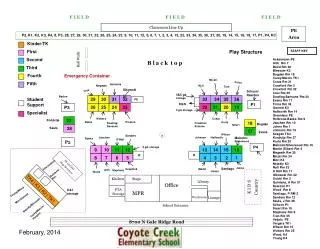
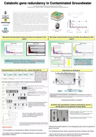
Download
1 / 16
180 likes | 233 Vues
(F E D) FIELD EMISSION DISPLAY. DEEPAK GUPTA EC 3 rd YR. 0800131034. PLAN OF PRESENTATION. WHAT WHEN APPS. HOW ADV. CHARACTERISTICS. FED.

E N D
(F E D)FIELD EMISSION DISPLAY DEEPAK GUPTA EC 3rd YR. 0800131034
PLAN OF PRESENTATION WHAT WHEN APPS. HOW ADV. CHARACTERISTICS
FED • FED is such a display that works a bit like a cathode-ray tube, except that electrons are emission procedure • Instead of one cathode emission spraying of electron through number of hole is done
HISTORY • In 1968, Charles A. "Capp" Spindt at the Stanford Research Institute had the idea of fabricating a flat display using microscopic molybdenum cones singly or in arrays (FEA’s) • This development was the enabling technology the concept for using FEA’s in a matrix addressed display (FED)
Field emission displays, electrons coming from millions of tiny microtips pass through gates and light up pixels on a screen.This principle is similar to that of cathode-ray tubes in television sets. The difference: Instead of just one "gun" spraying electrons against the inside of the screens face, there are as many as 500 million of them . FED Principles
Cathode The cathode/back plate is a matrix of row and column traces. Each crossover lays the foundation for an addressable cathode emitters. Each crossover has up to 4,500 emitters, 150 nm in diameter. This emitter density assures a high quality image through manufacturing redundancy, and long-life through low operational stress.
Emission Emitters generate electrons when a small voltage is applied to both row (base layer) and column (top layer).
FED PACKAGING • The field emission display screens are comprised of a thin sandwich. In this the back is a sheet of glass or silicon that contains millions of tiny field emitters which is the cathode. The front is a sheet of glass coated with phosphor dots, which is the anode.
FED CHARACTERISTICS • Comparing with the CRT displays the field emission displays has many advantages. • They are:
Brightness • 2. Speed • 3. Compact and lightweight • 4. Display size • 5. Low driving voltage • 6. Wider viewing angle • 7. High illumination • 8. Colour Quality
FED advantages Inherently high luminous efficiency No Response Time issues CRT-like Colour Gamut Lower Power Consumption Cold Cathode Emission Distance between cathode and screen ~0.2–5mm Flat Panel Technology Matrix Addressed – No DY Capital investment for manufacturing VLS TV with printable CNT FEDs - 1/10th of LCD Cost advantage over LCD could be 40%
APPLICATION This technology could produce affordable large displays in the 20 to 40-inch diagonal range suitable for TVs.
DRAWBACKS a. Vacuum tubes do require maintenance. b. Current FEDs often suffer from variation in screen brightness across the display, and also within each pixel. c. Durability due to electrical discharge in the small gaps everywhere in FED prototypes. d. The killing problem was durability: the tips could not survive under severe conditions of arcing (i.e. electrical discharge) due to the small gaps everywhere in FED prototypes.