Download
1 / 12
130 likes | 271 Vues
APV25 Thinning & Origami Status. M.Friedl, C.Irmler HEPHY Vienna. APV25 Purchase. Current Belle purchase 1500 diced „normal“ APV chips (~300µm thick) 2500 uncut APV wafers (for thinning) Future order 1000 more „normal“ APVs which did not fit in current purchase due to financial limits.

E N D
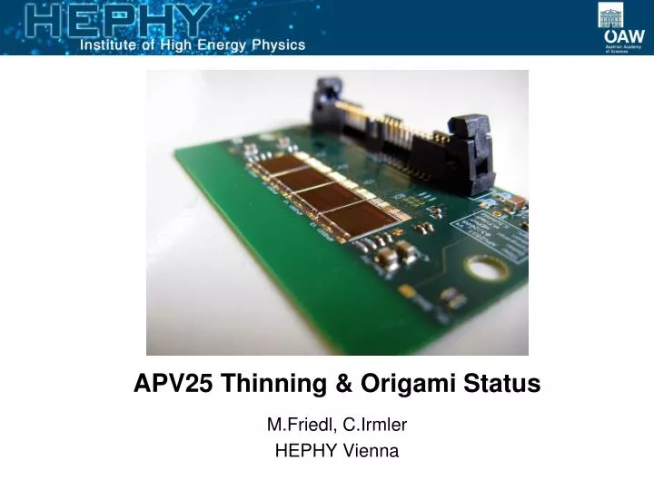
APV25 Thinning & Origami Status M.Friedl, C.Irmler HEPHY Vienna
APV25 Purchase • Current Belle purchase • 1500 diced „normal“ APV chips (~300µm thick) • 2500 uncut APV wafers (for thinning) • Future order • 1000 more „normal“ APVs which did not fit in current purchase due to financial limits • 8 wafers with a total of 2674 known good dies were delivered to Vienna on 9 Jan 2009 • One wafer contains 360 APVs in total • Each chip was tested on the wafer, yielding an average of 93% good dies • The 1500 normal APVs are on their way to KEK Markus Friedl (HEPHY Vienna)
APV25 Wafer Inspection APV25 wafers (8") Wafer map showing test results (used to ink mark bad dies on wafer) More photos: http://www.hephy.at/gallery2/v/electronics2/8inchwafer Markus Friedl (HEPHY Vienna)
APV25 Thinning • French company EDGETEK / WSI (http://www.edgetek.fr) • On 19 Jan 2009, we sent 1 wafer (319 good dies) for • thinning to 100µm (nominal) • dicing • waffle packing • Received back on 4 Feb 2009 • 105µm (nominal) thickness • 314 good dies (5 lost = 98.4% yield) • 104 + 105 test structures • remaining skeleton Markus Friedl (HEPHY Vienna)
Inspection of Thinned APVs Thickness measurement(Mitutoyo CMM) Waffle-packed thinned APV chips More photos: http://www.hephy.at/gallery2/v/electronics2/1stwaferthinned Markus Friedl (HEPHY Vienna)
Mechanical Investigation • Thickness measured on a total of 6 bad dies from various locations on the wafer skeleton • Table flatness +/- 3 µm • Thickness result: 106.6 +/- 3.2 µm 4 • Thin dies are still quite rigid • Handling is easier than expected • Thinning is mechanically OK Markus Friedl (HEPHY Vienna)
Functional Testing • 16 thinned APVs (~5% of all thinned chips) mounted onto 4 hybrids • 4 „normal“ APVs mounted onto 1 hybrid for comparison Markus Friedl (HEPHY Vienna)
Electronic Investigation • Comparing signal and noise of 20 APV chips • All hybrids show similar signal (internal calibration) and noise figures as well as current consumption 4 • S/N of naked hybrid (no fanout or sensor attached) is 57.9 +/- 5.5 • Variations are mostly attributed to channel-to-channel spread in readout system (hybrids connected to different channels in parallel ) • Apparently thinning has no effect on operation • All tested chips are fully functional • Thinning is electrically OK Markus Friedl (HEPHY Vienna)
Origami Concept • Extension of chip-on-sensor to double-sided readout • Flex fan-out pieces wrapped to opposite side (hence “Origami“) • All chips aligned on one side single cooling pipe Side View (below) Markus Friedl (HEPHY Vienna)
Origami Layout – Final Layout Connectors (on both sides) 2 p-side APV chips 2 p-side APV chips • 3-layer flex hybrid design • p- and n-sides are separated by 80V bias • n-side pitch adapter is integrated in hybrid • ordered at CERN PCB workshop, expected back ~end of March 4 n-side APV chips Animal farm (mascots:cat MF, eagle SS, bat CI) Flex fanouts to be Wrapped around the sensor edge Markus Friedl (HEPHY Vienna)
3D Rendering (readout connections not shown) • Will be equipped with 8 thinned APVs • Now designing jigs for assembly Markus Friedl (HEPHY Vienna)
Summary & Outlook • APV Thinning • 1st wafer successfully thinned & diced • Thickness of 106.6 µm achieved • Electric sample (~5%) tests perfectly fine • 8 more thinned APVs will be tested on Origami • Remaining APV wafers to be processed thereafter • Origami Status • flex circuit design submitted for fabrication at CERN, expected back ~end March 2009 • Jig design underway • We will assembe the first Origami module in April 2009 Markus Friedl (HEPHY Vienna)


![DNA origami attachment and AFM imaging on mica and SiO 2 /Si [100] in air](https://cdn1.slideserve.com/1982098/dna-origami-attachment-and-afm-imaging-on-mica-and-sio-2-si-100-in-air-dt.jpg)