Download
1 / 30
300 likes | 452 Vues
Development of a Silicon Tracking and Vertex Detection System for the CBM Experiment at FAIR. Johann M. Heuser, GSI Darmstadt, Germany for the CBM Collaboration VERTEX 2006, Perugia, Italy, September 2006. The international F acility for A ntiproton and I on R esearch

E N D
Development of a Silicon Tracking and Vertex Detection System for the CBM Experiment at FAIR Johann M. Heuser, GSI Darmstadt, Germany for the CBM Collaboration VERTEX 2006, Perugia, Italy, September 2006 • The international Facility for Antiproton and Ion Research • The Compressed Baryonic Matter experiment • The Silicon Tracking and Vertex Detection System: • Performance requirements, Detector concept, R&D activities J.M. Heuser CBM Silicon Tracking and Vertex Detection System
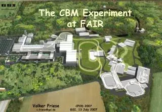
Observers: Facility for Antiproton and Ion Research @ GSI Darmstadt FAIR 2015 existing GSI Start of construction: 2007/2008 staged commissioning: 2011-2014 Full operation, CBM: 2015 International project: J.M. Heuser CBM Silicon Tracking and Vertex Detection System
Five Research Communities at FAIR Heavy-ionsynchrotrons Ion source SIS-100, SIS-300 SIS-18 U 35 GeV/n p 90 GeV Unilac CBM Nuclear Matter Physics with HI beams, 35-45 GeV/n, x1000 HESR Rare Isotope Prod. Target Super FRS Antiproton Prod. Target Hadron Physics with antiprotons 0 - 15 GeV Nuclear Structure & Astrophysics withradioactive beams, x10 000 and excellent cooling FLAIR CR- RESR Plasma Physics: x600 higher target energy density 600kJ/g NESR High EM Field(HI) _ Fundamental Studies(HI & p) Applications (HI) 100 m J.M. Heuser CBM Silicon Tracking and Vertex Detection System
Compressed Baryonic Matter-Experiment SIS-300: up to U92+,15-35 GeV/nucleon, beam intensities up to 109/s, Z/A = 0.5 nuclei up to 45 GeV/nucleon → exploration of the QCD phase diagram with heavy-ion collisions! → investigation of nuclear matter at highest baryon densities but still moderate temperatures in A+A collisions J.M. Heuser CBM Silicon Tracking and Vertex Detection System
CBM – Physics Case • Milestone in mapping the QCD phase diagram would be the (unambiguous) discovery of either the critical point or the 1st order phase transition • Top-energy SPS, RHIC, LHC : • high T, low mB region – • most probably phase crossover • High mB region ! • - onset of deconfinement? • - 1st order phase transition? • - critical point? • Earlier experiments: at AGS, low-energy SPS: • limited in observables, statistics • New : RHIC plans low energy runs SIS 300 @ FAIR: ideal for 2nd generation experiment! CBM: rare probes, high interaction ratescharm, dileptons, fluctuations, correlations J.M. Heuser CBM Silicon Tracking and Vertex Detection System
CBM collaboration Korea: Korea Univ. Seoul Pusan National Univ. Norway: Univ. Bergen Germany: Univ. Heidelberg, Phys. Inst. Univ. HD, Kirchhoff Inst. Univ. Frankfurt Univ. Kaiserslautern Univ. Mannheim Univ. Münster FZ Rossendorf GSI Darmstadt Poland: Krakow Univ. Warsaw Univ. Silesia Univ. Katowice Nucl. Phys. Inst. Krakow* Portugal: LIP Coimbra > 40 institutions > 350 Members Croatia: RBI, Zagreb China: Wuhan Univ. Hefei Univ. Cyprus: Nikosia Univ. Czech Republic: CAS, Rez Techn. Univ. Prague France: IReS Strasbourg Hungaria: KFKI Budapest Eötvös Univ. Budapest India: VECC Kolkata IOP Bhubaneswar* Univ. Chandighar* Univ. Varanasi* Romania: NIPNE Bucharest Russia: IHEP Protvino INR Troitzk ITEP Moscow KRI, St. Petersburg Kurchatov Inst., Moscow LHE, JINR Dubna LPP, JINR Dubna LIT, JINR Dubna MEPHI Moscow Obninsk State Univ. PNPI Gatchina SINP, Moscow State Univ. St. Petersburg Polytec. U. Ukraine: Shevshenko Univ. , Kiev * to be approved by CB open for new partners! J.M. Heuser CBM Silicon Tracking and Vertex Detection System
The CBM Experiment • tracking, momentum, vertex reconstruction: silicon pixel/strip detectors (STS) in magnetic dipole field • electron ID: RICH & TRD (& ECAL) • p suppression 104 • hadron ID: TOF (& RICH) • photons, p0, m ID: ECAL • event characterization (PSD) • high speed DAQ, only high-level triggers • not necessarily fixed layout! • more like „facility“ J.M. Heuser CBM Silicon Tracking and Vertex Detection System
Alternative CBM setup: Dimuons • Dimuon setup studied with active muon absorbers (Fe + C + detector layers) after the Silicon Tracker • ... move absorbers out for hadron runs. J.M. Heuser CBM Silicon Tracking and Vertex Detection System
Silicon Tracking and Vertexing • Challenge:Au+Au collisions, 25 GeV/n: • high track densities: • 600 charged particles in 25o • high r/o speed, radiation hardness: 10 MHz interaction rate (109 ions/s on 1% int target), only high-level triggers. • Tasks: • track reconstruction for particles with 0.1 GeV/c < p 10-12 GeV/c , momentum resolution ~ 1% at 1 GeV/c,large lateral coverage • primary and secondary vertex reconstruction (resolution 50 mm) • V0 track pattern recognition (low-mass vector mesons lepton pairs, open charm decays, hyperons, e+e- pairs from g-conversion) D+→ p+p+K- (ct = 317 mm) D0 → K-p+ (ct = 124 mm) J.M. Heuser CBM Silicon Tracking and Vertex Detection System
STS VTS 25º 2.5º vacuum Conceptional Detector Geometry Vertexing: "VTS" 2 (3) MAPS stations. z = (5), 10, 20 cm 150 µm Si In vacuum. No layout yet. Tracking: "STS" 2 HYBRID Pixel stations: z = 30, 40 cm 750 µm Si No layout yet. 4 Micro-STRIPS stations: z = 50, 60, 75, 100 cm 400 µm SiDetailed station layout. very thin low-mass J.M. Heuser CBM Silicon Tracking and Vertex Detection System
GEANT implementation: • dipole magnet, • 1Tm bending power • VTS in vacuum section • beam pipe • STS stations 1 m Activities started on:optimization of layout, robust tracking, vertexing, detector/system R&D J.M. Heuser CBM Silicon Tracking and Vertex Detection System
detector module r/o electronics r/o sensors Microstrip Tracking Stations Sensor arrangement and hit digitization scheme. Old concept: "radial" arrangement of sectors New concept: double-sided sensors50 µm strip pitch, 15 deg stereo angle strip lengths 4-12 cmr/o through thin, long analog cables ! J.M. Heuser CBM Silicon Tracking and Vertex Detection System
detector module r/o electronics sensors Microstrip Stations: conceptional structure Station 5z = 50 cm Station 6z = 60 cm Station 8z = 100 cm Station 7z = 75 cm J.M. Heuser CBM Silicon Tracking and Vertex Detection System
standard thick-3 thick-2 thick thin Momentum Resolution Thickness:effective,sensor + support/cables. How much passive material (support, cables etc) will finally add up? Readout: What sensor thickness for what S/N? Detailed simulations being prepared. Study impact on physics. thin: standard: thick: thick-2: thick-3: MAPS2×150 µm 2×150 µm2×150 µm 2× 150 µm 2× 150 µmHybrid2×200 µm 2×750 µm 2×800 µm 2×1000 µm 2×1600 µm Strips4×200 µm 4×400 µm 4×800 µm 4×1000 µm 4×1600 µm J.M. Heuser CBM Silicon Tracking and Vertex Detection System
all reconstructed tracks primary tracks 92.17 ± 0.14 97.02 ± 0.09 Track Reconstruction Efficiency Track finder: Cellular Automaton and Kalman Filter: - with 2 Hybrid Pixel + 4 Strip Stations, - standard settings: include vertex, hits in >3 consecutive stations. J.M. Heuser CBM Silicon Tracking and Vertex Detection System
standard detector configuration: L1 tracking with 2 Hybrid pixel + 4 Strip Stations 2 Strip Stations (avoid 2nd technology) primary tracks all reconstructed tracks 94.88 ± 0.12 90.01 ± 0.15 Microstrip-Only Track Reconstruction What's the design goal? Important: Include robustness! J.M. Heuser CBM Silicon Tracking and Vertex Detection System
xy+uv Frontal view Side view xy uv robust "space points" Tracking with four strip projections per station: Microstrip-only tracker Tracking: double stations strips Vertexing with 2 MAPS stations: either: at 5 cm + 10 cm, or: at 10 cm + 15 cm. J.M. Heuser CBM Silicon Tracking and Vertex Detection System
Microstrip Double-Stations -3.75o xy uv 3.75o 0o 3.75o -3.75o -11.25o 11.25o Δz 1 cm 4 hit projections on the strip planes J.M. Heuser CBM Silicon Tracking and Vertex Detection System
Tracking Stations: Layout Studies Occupancies: Up to 5% in hottest sectors of station 5 (central collisions). Go down with radial distance from the beam axis, and with distance from the target ...... as expected. The CA track finder yields tracking efficiencies ~97%. Together with tracking study: powerful design tool. Design criteria: - Save r/o channels in outer regions: Longer strips there! - Short strips close to beam line. J.M. Heuser CBM Silicon Tracking and Vertex Detection System
LY I II LX Microstrip Sensor Development r/o direction Two streams of activities: double-sided, different technologies 1) In CBM Collaboration (R&D at MSU SiLab, Moscow) 300 µm, polysilicon biassing, p-stop connectivity: top/bottom + sides 2) R&D at GSI, together with CIS, Germany 300 µm, punch-through biassing, p-spray, double-metal connectivity: r/o at top/bottom edge n side:"vertical" strips p side: "stereo" strips r/o direction n side:"vertical" strips p sidewith "double metal" blue:double metal connections of strips in regions I to III III J.M. Heuser CBM Silicon Tracking and Vertex Detection System
256 x 256 strips80 µm pitch90 deg stereo angle 256 x 256 strips50 µm pitch90 deg stereo angle 1024 x 1024 strips50 µm pitch15 deg stereo angle 4" wafer, 280 µm thick design finished design finished design partlyfinished R&D with CIS Erfurt, Germany: (http://www.cismst.de/english/frameset.html) CBM: Opportunity to participate in reseach project of CIS (focus on rad hard detectors). CBM sensor prototypes as "test objects". Sensor design: finished 10/2006.End 2006: batch of ~ 20+ wafers. Plenty of sensors for a variety of tests of r/o electronics and detector concept. Set up Silicon labs at GSI + other institutes. Test beam + telescope at GSI. J.M. Heuser CBM Silicon Tracking and Vertex Detection System
Microstrip Detector Readout Two streams of activities: 1) In the CBM Collaboration (MEPhi/MSU, Moscow): R&D on fast self-triggered low-power electronics blocks 2) Exploration of the NXYTER chip in collaboration with the Consortium DETectors for Neutron Imaginghttp://jra1.neutron-eu.net/jra1 • dual polarity • input pitch: 50.7 µm • 128 channels per chip • amplitude measurement • data driven token-ring r/o architecture • count rates: ~160 kHz/strip • charge collection 30 ns peaking time • small (~2 ns) timing jitter • thresholds: > 2700 e • dynamic range: different for +/- • power: ~ 13 mW/channel (high!!!) • produced in 0.35 m CMOS Specs very similar to the CBM needs! 1st chip submission in March 2006. • Close ties to the project through Head of GSI Detector Lab • GSI: significant participation in funding of chip submission (Summer 2006). Aim: Test and modify this chip. Construction of a demonstrator microstrip detector module for CBM. J.M. Heuser CBM Silicon Tracking and Vertex Detection System
N-XYTER Submitted via CMP Dies Expected Sept. 25th 2006 8 LVDS output lines at 4 x 32MHz: time stamp, channel no. + 1 differential, analog output 128 analog inputs poisson distributed at 32 MHz total average input rate AMS CMOS 0.35µ with thick metal four J.M. Heuser CBM Silicon Tracking and Vertex Detection System
Study on Mechanical Structure Elements (microstrip module): 2-module structure, building block of detector stations Study together with ITEP Moscow: Based on ALICE ITS studies, and CBM STS layout concept.Carbon fibre. module "very preliminary, brain-storming designs" flat cable routing sensor holders J.M. Heuser CBM Silicon Tracking and Vertex Detection System
Vertex Tracking System • Sensor Requirements: • pitch 20 μm • thickness below 100 μm • single hit resolution : 3 μm • radiation tolerant, design goal 1013 neq/cm2 • ultimate read-out time 5-10 μs Hybrid pixels: at least for now: - too thick- too large pixels - power dissipation requires cooling. • Monolithic Active Pixel Sensors (MAPS) • R&D together with IPHC (IReS) Strasbourg • development of fast column//architecture • development of radiation tolerant sensors (from some 1012 to 1013neq /cm2) SOI pixels: in a small process: interesting! MAPS with depletion layer: sounds interesting! longer lifetime of first MAPS station: enlarge distance from target: 5 cm → 10 cm J.M. Heuser CBM Silicon Tracking and Vertex Detection System
R&D goals with MAPS: Radiation tolerance & readout speed R&D goals with MAPS: radiation tolerance: ~1012 1013 1 MeV nequiv. readout time: 10 sec, column parallel r/o Expected situation in CBM: Fluence at 1st MAPS station: ~10 1-MeV nequiv. per event detector partly destroyed after 1012 reactions corresponds to 105 D mesons detected (already decent measurement!) Possible running conditions: a)1 day detector lifetime at 107 reactions/s,100 events piled up, or b) 4 month detector lifetime at 105 reactions/s, no pile-up events. URQMD, Au+Au 25 GeV/nucleon Fluence of 1 MeV nequiv./cm2in 1st MAPS station at z = 5cm Kpn What about retracting the 1st MAPS station from the target? J.M. Heuser CBM Silicon Tracking and Vertex Detection System
Benchmark for SVT and STS Performance: D0 mesons, Au+Au collisions at 25 AGeV 1st MAPS station at z = 5 cm 1st MAPS station at z = 10 cm D0 S/B = 3.5 • realistic tracking in magnetic field, • 2 MAPS, 2 Hybrid pixel, 4 Strip stations • proton identification required • D0 production cross section from HSD • 25 AGeV Au+Au from UrQMD • minimum bias collisions dose × ¼ S/B × ¼ no gain!! J.M. Heuser CBM Silicon Tracking and Vertex Detection System
Summary - CBM • CBM is a baseline experiment at FAIR. Running from 2014/15. • CBM offers very interesting physics program on the QCD phase diagram. • Unique features expected in CBM energy range: First order phase transition, critical point • As a 2nd generation experiment, CBM will be able to study: rare probes, fluctuations and correlations! • Detector development under way • Increasingly realistic feasibility studies are performed • → Technical Proposal in ~2007. J.M. Heuser CBM Silicon Tracking and Vertex Detection System
Summary – Silicon Detectors The Silicon Tracking and Vertex Detection System is the core of CBM. Detector concept: Tracker (Microstrips) + Vertex Detector (MAPS) R&D activities: - layout optimization: Ongoing. New and powerful tools available for realistic detector/physics simulations. - tracking studies: Ongoing - sensor development: Ongoing - r/o electronics development: Ongoing - mechanical studies: Beginning Still may gaps to fill, including: - realistic sensor shapes, support material in simulations. - realistic FLUKA radiation study. - R&D on module prototypes: Microstrips & MAPS. - thin sensors, low-mass r/o cables, low-mass support structures. - ... J.M. Heuser CBM Silicon Tracking and Vertex Detection System
Data-Push Architecture, Data Flow • Each detector channel detects autonomously all hits FEE design. • An absolute time stamp, precise to a fraction of the sampling period, is associated with each hit. • All hits are shipped to the next layer (usually data concentrators). • Association of hits with events done later using time correlation. Typical parameters: (few % occupancy, 107 interaction rate) • some 100 kHz hit rate per channel • few MByte/sec per channel • whole CBM detector: ~ 1 Tbyte/sec J.M. Heuser CBM Silicon Tracking and Vertex Detection System