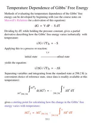
Download
1 / 22
360 likes | 818 Vues
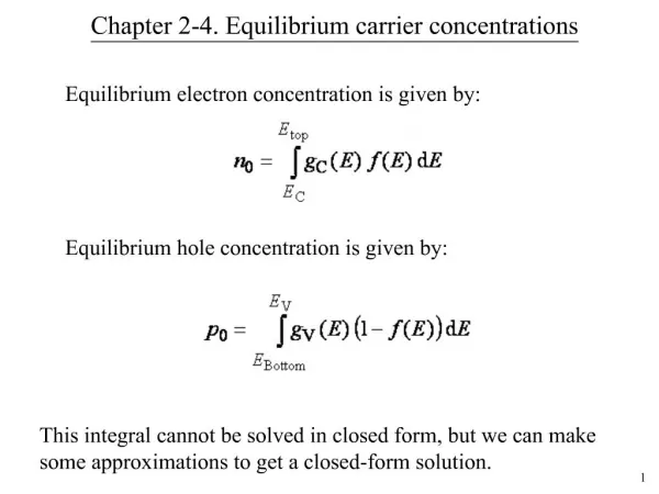
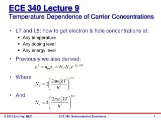
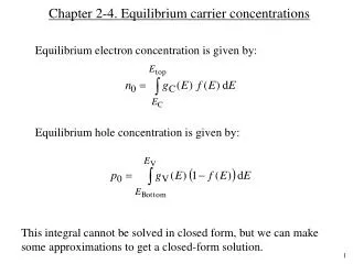
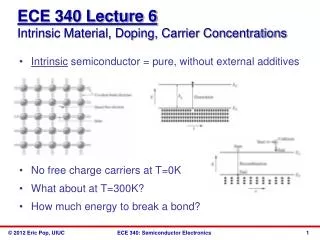
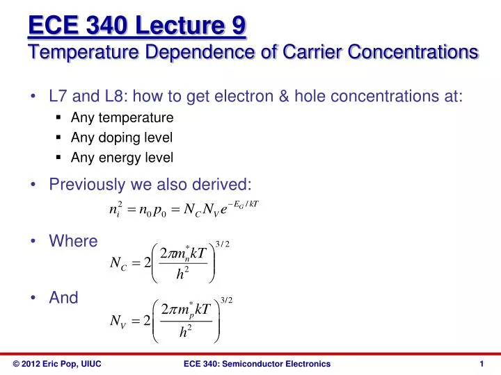
ECE 340 Lecture 9 Temperature Dependence of Carrier Concentrations. L7 and L8: how to get electron & hole concentrations at: Any temperature Any doping level Any energy level Previously we also derived: Where And. So the intrinsic carrier concentration at any T is:

E N D
ECE 340 Lecture 9Temperature Dependence of Carrier Concentrations • L7 and L8: how to get electron & hole concentrations at: • Any temperature • Any doping level • Any energy level • Previously we also derived: • Where • And
So the intrinsic carrier concentration at any T is: • What does this tell us? • Note that mn*=1.1m0 and mp*=0.56m0 • These are ________________________ effective masses in Si, not to be confused with _______________________ • Does the band gap EG change with T?
Plot log10 of ni vs. T • What do we expect? • Note your book plots this vs. 1000/T in Fig. 3-17; why? • What is this (simple) plot neglecting?
Recall ni is very temperature-sensitive! Ex: in Silicon: • While T = 300 330 K (10% increase) • ni = ~1010 ~1011 cm-3 (10x increase) • Also note: • Now we can calculate the equilibrium electron (n0) and hole (p0) concentrations at any temperature • Now we can calculate the Fermi level (EF) position at any temperature • Ex: Calculate and show position of Fermi level in doped Ge (1016 cm-3 n-type) at -15 oC, using previous plot
Assume Si sample doped with ND = 1015 cm-3 (n-type) • How does n change with T? (your book plots this vs. 1000/T in Fig. 3-18) • Recall the band diagram, including the donor level. • Note three distinct regions: • Low, medium, and high-temperature
So far, we assumed material is either just n- or p-doped and life was simple. At most moderate temperatures: • n0 ≈ • p0 ≈ • What if a piece of Si contains BOTH dopant types? This is called compensation. • Group V elements are _______ and introduce ________ • Group III elements are _______ and introduce ________
Case I, assume we dope with ND > NA • Additional electrons and holes will _____________ until you have n0 ≈ ND - NA and p0 ≈ _________ • Case II, what if we introduce ND = NA dopants? • The material once again becomes ____________ and n0 ≈ p0 ≈ ______ • Case III and more generally, we must have charge neutrality in the material, i.e. positive charge = negative charge, so p0 + ND = __________
So most generally, what are the carrier concentrations in thermal equilibrium, if we have both donor and acceptor doping? • And how do these simplify if we have ND >> NA (n-type doping dominates)? • When is “>>” approximation OK?
ECE 340 Lectures 10-11Carrier drift, Mobility, Resistance • Let’s recap 5-6 major concepts so far: • Memorize a few things, but recognize many. • Why? Semiconductors require lots of approximations! • Why all the fuss about the abstract concept of EF? • Consider (for example) joining an n-doped piece of Si with a p-doped piece of Ge. How does the band diagram look?
So far, we’ve learned effects of temperature and doping on carrier concentrations • But no electric field = not useful = boring materials • The secret life of C-band electrons (or V-band holes): they are essentially free to move around, how? • Instantaneous velocity given by thermal energy: • Scattering time (with what?) is of the order ~ 0.1 ps • So average distance (mean free path) travelled between scattering events L ~ _______
But with no electric field (E=0) total distance travelled is: ___ • So turn ON an electric field: • F = ± qE • F = m*a a = • Between collisions, carriers accelerate along E field: • vn(t) = ant = ______________ for electrons • vp(t) = apt = ______________ for holes • Recall how to draw this in the energy band picture
On average, velocity is randomized again every τC (collision time) • So average velocity in E-field is: v = _____________ • We call the proportionality constant the carrier mobility • This is a very important result!!! (what are the units?) • What are the roles of mn,p and τC?
Then for electrons: vn = -μnE • And for holes: vp = μpE • Mobility is a measure of ease of carrier drift in E-field • If m↓ “lighter” particle means μ… • If τC↑ means longer time between collisions, so μ… • Mobilities of some undoped (intrinsic) semiconductors at room temperature:
What does mobility (through τC) depend on? • Lattice scattering (host lattice, e.g. Si or Ge vibrations) • Ionized impurity (dopant atom) scattering • Electron-electron or electron-hole scattering • Interface scattering • Which ones depend on temperature? • Qualitative, how? • Strongest scattering, i.e. lowest mobility dominates.
Qualitatively • Quantitatively we rely on experimental measurements (calculations are difficult and not usually accurate): http://www.ioffe.rssi.ru/SVA/NSM/Semicond/Si/electric.html
Once again, qualitatively we expect the mobility to decrease with total impurities (ND+NA) • Why total impurities and not just ND or NA? (for electrons and holes?)
Ex: What is the hole drift velocity at room temperature in silicon, in a field E = 1000 V/cm? What is the average time and distance between collisions?
Now we can calculate current flow in realistic devices! • Net velocity of charge particles electric current • Drift current density ∝ net carrier drift velocity ∝ carrier concentration ∝ carrier charge • First “=“ sign always applies. Second “=“ applies typically at low-fields (<104 V/cm in Si) (charge crossing plane of area A in time t)
Check units and signs: • Total drift current: • Has the form of Ohm’s Law! • Current density: • Current: • This is very neat. We derived Ohm’s Law from basic considerations (electrons, holes) in a semiconductor.
Resistivity of a semiconductor: • What about when n >> p? (n-type doped sample) • What about when n << p? (p-type doped sample) • Drift and resistance:
Experimentally, for Si at room T: • This is absolutely essential to show our control over resistivity via doping! • Notes: • This plot does not apply to compensated material (with comparable amounts of both n- and p-type doping) • This plot applies most accurately at low-field (<104 V/cm)