Download
1 / 38
450 likes | 777 Vues
Flash Memory Built-in Self-Test with Enhanced Test Mode Control. Advisor: Cheng-Wen Wu, Ph.D. Student: Yan-Ting, Lai June 3, 2004. Outline. Introduction Flash Memory Testing Issues Flash Memory Built-in Self-Test Issues Proposed BIST Design Experimental Results and Prototyping System

E N D
Flash Memory Built-in Self-Test with Enhanced Test Mode Control Advisor: Cheng-Wen Wu, Ph.D. Student: Yan-Ting, Lai June 3, 2004
Outline • Introduction • Flash Memory Testing Issues • Flash Memory Built-in Self-Test Issues • Proposed BIST Design • Experimental Results and Prototyping System • Conclusion
USB driver Introduction (1/2) • Flash memory is a type non-volatile memory which can be programmed or erased electrically • Flash memory is widely used in many applications such as DSC, cell phone, USB driver, etc. DSC Cell-phone
Introduction (2/2) • The basic operations of Flash memory are Read, Program and Erase
Flash Memory Testing Issues • Reliability issues • Disturbances • Over-erasing • Endurance • Retention • Ad-hoc test can’t provide sufficient fault coverage • Long program/erase time • Test access issues for embedded Flash memory • High ATE cost, and grows rapidly with memory performance improvement
Solutions • Reasonable fault models • Model reliability-related defects • Efficient test algorithms • Provide easy implementation • Reduce test time • Increase fault coverage • Built-in self-test (BIST) circuit for Flash memory • Replace or reduce the requirement of ATE • Reduce the complexity of test flow • “Built-in Self-Test and Built-in Self-Repair will be essential to test embedded memories and to maintain production throughput and yield” [ITRS 2003]
Previous BIST for Flash Memory (1/3) • V. Mastrocola proposed a BIST design for low cost testing of a stand alone Flash memory • This BIST is realized by using LFSR with internal address counter and clock available in Flash memory • Burst read operation is used to reduce the read time • At-speed testing at 60Mhz and maximum test coverage using a low cost ATE is possible • The feedback polynomial can be selected during testing Source: V. Mastrocola et al., IOLTW01
Previous BIST for Flash Memory (2/3) • P. Bernardi presented a P1500-compatible programmable BIST for embedded Flash memory • A custom processor wrapper is used to provides low area overhead, wiring cost and high flexibility • The designed instruction set allows the processor to execute the March-like algorithms • The efforts to modify test program and the test architecture for different flash models are reduced by using this method Source: P. Bernardi et al., DATE03
Previous BIST for Flash Memory (3/3) • J.C. Yeh proposed March-FT algorithm to cover all the disturbance faults and traditional RAM functional faults • S.K. Chiu proposed Diagonal test scheme to reduce the test time • The above researchers also presented a BIST design using their proposed algorithms • Y.Y. Shih proposed a BIST circuit design to suit for the Hi-V operation of flash memory and provide a low cost diagnosis system Source: J.C. Yeh et al., DELTA02 Source: S.K. Chiu et al.,ITC02 Source :Y.Y. Shih’s thesis
Flash Memory BIST Issues • Various Flash memory architectures • Built-in Self-Test and Built-in Self-Diagnosis • Test flow simplification • Programmability for flexibility • Test pin reduction • Test time reduction • Device protection
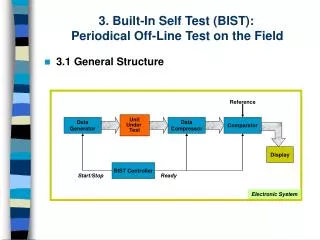
Approaches for Flash memory BIST • A flexible BIST architecture can be used with the modification of test pattern generator (TPG) • BIST & BISD are both needed or integrated • Supports Burn-in or Cycling test to reduce test complexity • On-line programmable • Use fewer I/O to reduce ATE pin cost • Utilization of engineering test mode to reduce test time • Device protection function
BIST Functions • Three modes • Test Mode : Test with built-in test algorithm • Diagnosis Mode : Test with shift-in algorithms • Burn-in Mode : Cycling read through all addresses • Three kinds report methods • “Go/No-Go” • “Error Information for Repair” (EIR) • “Error Information for Diagnosis” (EID) • Reset wait function
Flash Memory Target Faults • Disturb Faults: • Program Disturbance • Word-line Program Disturbance (WPD) • Word-line Erase Disturbance (WED) • Bit-line Program Disturbance (BPD) • Bit-line Erase Disturbance (BED) • Read Disturbance (RD) • Over Erase/Program (OE/OP) Faults • Conventional RAM Faults • SAF, TF, SOF, AF, CFst Source: J.C. Yeh et al. ,DELTA02
Support Test Algorithms • Test Mode • March-FT (built-in test algorithm) • (f); ↑(r1,p0,r0);↑(r0); (f); ↓(r1,p0,r0); ↓(r0); • In Diagnosis Mode, we can shift-in any combinations of our defined test commands as user-defined test algorithms • March-FD (recommended) • (f); ↑(r1); ↑(r1,p0,r0); (f); ↑(r1);↓(r1,p0,r0,r0); ↑(r0,p0); ↑(r0); • MSCAN (recommended) • (f); ↓(r1); ↓(p0); ↓(r1); • Burn-in Mode • ↑(r1); ↑(r0); ↓(r1); ↓(r0); ↑(r1); ↓(r0); ↓(r1); ↑(r0);
Command Format 4 2 1 0 CMD DBG DIR CMD: Algorithm Elements & BIST Operation DBG: Data Background DIR : Address Direction
Test Time Evaluation by RAMSES-FT Source: K.L Cheng et al. ,VTS02 FLASH memory simulator. This memory is NAND type (BiAND gate). Memory block size : 16896x8 (16KByte) Row x Col : 16x8448 Test length : 2(erase_time) + 64(page_program_time) + 192(page_read_time) Test time : 23.7792 msec / block Fault coverage : BPD : 1.0 WPD : 1.0BED : 1.0 WED : 1.0RD : 1.0 OE : 1.0SAF : 1.0 TF : 1.0SOF : 1.0 CFst : 0.99829018116AF : 0.99658036232 Total Blocks: 2048 Total test : 23.7ms x 2048= 48.72s E: 2ms Page_P: 200us Page_R: 10us+50ns*527 =36.35us
Reduced Test Time Time Specification Total Test Time for Whole Chip Test time improvement = 35.6%
Error Format Err Syndrome Err Address d0 a24 a0 d15 Err Syndrome : Error syndrome information Err Address : Faulty address information Total Shift-Out Cycles = 41 Err Address Err Section Err Syndrome e0 d15 a24 e4 d0 a0 Err Section : Indicate which operation reads fault Err Syndrome : Error syndrome information Err Address : Faulty address information Total Shift-Out Cycles = 46
EIR Shift-Out Cycles Overall Shift-Out Cycles Reduction Ratio ≈ 80%
Original Flash Memory Design BIST Combined with Flash Memory
Test Mode Simulation Result Flash (w1) (r1,p0,r0) (r1)
Diagnosis Mode Simulation Result Shift OutCycles FaultFree
Hardware Overhead Estimation • Due to the canceling of this project, we used TSMC 0.35 um CMOS technology instead of EMTC’s library to do estimation
Flash memory in Socket & FPGA PC Logic Analyzer Data Log or Direct Access Configure FPGA Error Log Analysis Prototyping System
Prototyping Results • We have three test chips to verify our design • The ATE’s results about chip2 and chip3 fail is due to the fail of I/O open/short test • Our prototyping system can access them all at a lower speed and get interesting results
Diagnosis Results for Chip2 Block 0 Block 0 Block 1 Block 1 Block 2 Block 2 Plane 1 Plane 0 Block 651 Block 1020 Block 1021 Block 1021 Block 1022 Block 1022 Block 1023 Block 1023
Conclusions • We proposed a programmable BIST design with enhanced test mode control for Flash memory whose area overhead is about 0.5% • The engineering test mode operations are used to reduce test time • Parallel shift-out mechanism is used to reduce unaccepted long shift-out cycles • Reset Wait function provides device protection • A low cost prototyping system for diagnosis is presented to reduce the diagnosis scheme cost
Future Work • Built-In Self-Redundancy Analysis (BIRA) is needed to support internal redundancy analysis and reduce shift-out cycles • In order to improve the yield, Built-In Self-Repair (BISR) should be developed • More efforts should be put on to construct a simple and effective Flash memory physical model to do failure analysis and memory diagnosis