Download
1 / 46
1.06k likes | 2.03k Vues
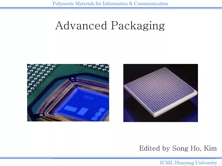
Advanced Packaging. Edited by Song Ho, Kim. Protection against heat. Main function Of packaging. protection. Good mounting. Electric connect. Main Functions of Semi-Conductor Packaging. Structure of Semi-Conductor. Types of Packaging. Trends of Packaging Materials.

E N D
Advanced Packaging Edited by Song Ho, Kim
Protection against heat Main function Of packaging protection Good mounting Electric connect Main Functions of Semi-Conductor Packaging
Multi-Functionalization A) MCM B) SIP C) SOP
Process of Semi-conductor Packaging(Back-end Process) 1) Lead Frame Materials : DRAM, Flash Memory, Sys.-LSI
Process of Semi-conductor Packaging(Back-end Process) 2) Substrate Materials : BOC, FBGA, MCP, MSP
Disintegration of IC design, fabrication, and packaging within OEMs and IDMs is creating a potential void in leadership for development of new packaging, materials, and process solutions. Who will carry the future development burden? Packaging Development Leadership
Advanced Packaging Innovation(1) • Systemic Innovation • - Innovation that can only be realized in conjunction with a complementary or related innovation • Silicon packaging challenges are getting more complex • -Substrate manufacture and materials • -Assembly process and materials • -thermal management • -Die stress(low-k and copper) • -Electrical performance
Advanced packaging Innovation(2) • Systemic innovation often requires scale, integration, and market leadership to drive new standards • -Example: Intel and IBM in CPUs • Ti in DSPs • RFMD and Conexant in Sip • Novel packaging innovation requires a sustained specific product focus to drive technical and commercial developement
Gross margins for advanced packaging assembly range from 10%-25%, and packaging R&D spending is generally less than 2% of sales for leading subcontractors. Focus of development is on process integration rather than fundamental materials or equipment innovation. To some degree, subcontractors continue to leverage supplier technology enabled by IDMs, and hire technical resources from captive suppliers. Outsource business models make the case that the separation of product innovation and manufacturing leads to lower costs and potentially faster product innovation. This is not always true, and particularly at the leading edge. IC Package Outsourcing Trends(1)
IC Package Outsourcing Trends(2) • For most leading IDMs, critical products still support significant investments in packaging technology development, along with the desire to maintain full control over packaging solutions, whether captive or merchant. • Silicon foundries are unlikely to expand packaging development beyond wafer level services(redistribution, bumping), but do see value in partnership with outside service providers, such as the major subcontract IC assemblers. They will play a role of “virtual” service provider. • While there is little, if any, profit in technology and service development for subcontractors, most of the leading players view the role of process integration as critical to their future.
Primarily Captive IDMs-Integrated Device Manufactures(Philips, ST, Agere) - Typically 0.4% to 0.5% of semiconductor revenues are used for package development, qualification, and move to production programs Primarily captive at high end, but use subcontractors otherwise (AMD, Intel, TI) 0.3% to 0.4% of revenues used for package development,etc. Subcontract Package Assemblers(Amkor, ASE, SPIL) 1.5% to 2.5% of revenues are for R&D Fabless Semiconductor Companies(Altera, VIA, Ali, SiS) - Less than 1% of employees are package related; very few, if any, in development Package Relater Engineering Resources(1)
Translates to relative spending IDMs: $500M-$600M per year Subcontract Assemblers: <$100M per year IDMs will continue to out-invest the merchant suppliers for many years to come, with a focus on leading edge products However, continuing margin erosion and increased outstanding by IDMs will likely reduce packaging development resources over time Package Relater Engineering Resources(2)
Wire Bond Progress Competition with Flip Chip Interconnection :
Conductors and dielectrics Local through global levels Associated planarization Necessary etch, strip and clean Embedded passives Reliability and system and performance issues Ends at the top wiring bond pads Interconnector Scope
Introduction of new materials Integration of new processes and structures Achieving necessary reliability Attaining dimensional control Manufacturability and defect management that meet overall cost/performance requirements * Top three grand challenges Dimensional control and metrology Patterning, cleaning and filling high aspect ratios features Integration of new processes and structures Continued introductions of new materials and size effects Identify solutions which address global wiring scaling issues Identify solutions which address global wiring scaling issues Difficult Challenges > 65mm < 65mm
Near term • new barriers and nucleation layers - in situ formed dielectric and metal • porous dielectrics • ALD potential solutions Combination of materials and technologies Many new reliability challenges • new materials and interfaces • electrical, thermal and mechanical exposure Introduction of New Materials
Long term - Continued introduction of materials • barriers/nucleation layers for alternate conductors - optical, low temp. RF, air gap • alternate conductors, cooled conductors - More reliability challenges - Microstructural and atom scale effects Materials Challenges
3DCD of features - performance and reliability implicatons Multiple levels - reduced feature size, new materials and pattern dependent processes - process interactions • CMP and deposition-dishing/erosion-thinning • Deposition and etch-to pattern multi-layer dielectrics • Aspect ratios for etch and fill - particularly DRAM contacts and dual damascene Dimensional Control
Combinations and interactions of new materials and technologies - interfaces, contamination, adhesion, diffusion, leakage concern, thermal budget, ESH, CoO Structural complexity - levels-interconnect, ground planes, decoupling caps - passive elements - mechanical integrity - other SOC interconnect design needs(RF) - cycle time Process Integration
Many new low and high k materials- may require new chemistries-supercritical CO2 /solvents, ozone gas/liquid approaches Strip/clean compatibility with these new materials Dimensional control with small features and high A/R Low damage MRAM, FeRAM, applications Etch, Strip and Clean Potential Solutions
CEP-chemically enchanced planarization and spin etch approaches Porous low k will require either alternative planarization or stopping layer/structural enhancements to be compatible with existing planarization technique Planarization Solutions
Paradigm Shift in Customer Requirement to Integrated Solution