Download
1 / 44
440 likes | 586 Vues
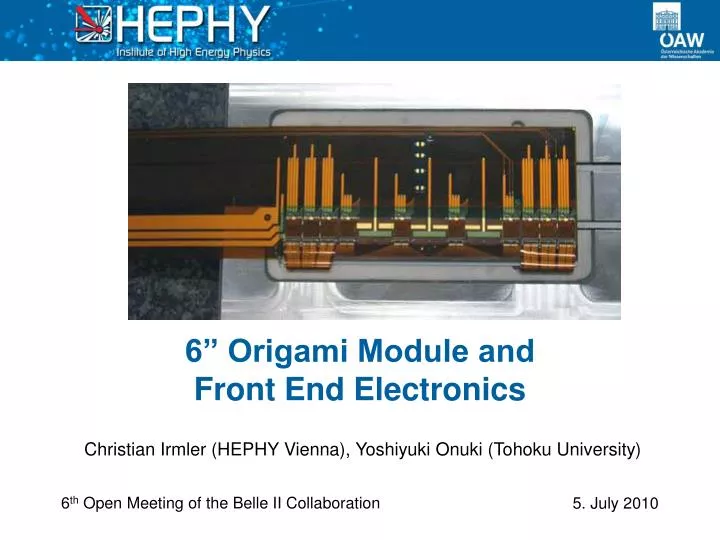
6” Origami Module and Front End Electronics. 6 th Open Meeting of the Belle II Collaboration. Components Testing & Quality Check Assembly Module Test Summary. Components Testing & Quality Check Assembly Module Test Summary. Origami Chip-on-Sensor Concept.

E N D
6” Origami Module and Front End Electronics Christian Irmler (HEPHY Vienna), Yoshiyuki Onuki (Tohoku University) 6th Open Meeting of the Belle II Collaboration
ComponentsTesting & Quality CheckAssembly Module TestSummary Christian Irmler (HEPHY Vienna), Yoshiyuki Onuki (Tohoku University)
ComponentsTesting & Quality CheckAssembly Module TestSummary Christian Irmler (HEPHY Vienna), Yoshiyuki Onuki (Tohoku University)
Origami Chip-on-Sensor Concept • Principalfeasibility shown in 2009 by building a prototype module using a 4” DSSD • Successfully tested in lab and SPS beam • Can it be scaled up to the size required for the center 6” sensor of the outer most ladder? Christian Irmler (HEPHY Vienna), Yoshiyuki Onuki (Tohoku University)
Summary 4” Origami • Flex hybrid produced by CERN PCB workshop • long delivery time • almost made by hand • not suitable for series production • Several vias broke after soldering of electronics components • Only moderate bondability • We found a Japanese company for production of new 6” design Christian Irmler (HEPHY Vienna), Yoshiyuki Onuki (Tohoku University)
Origami Design for Belle II SVD • Present design for center module of outermost ladder (6“ HPK sensors) • Consists of 4 parts: • Origami PCB (~ 450 mm long) • PA0: pitch adapter for n-side, glued onto hybrid • PA1, PA2: pitch adapters to connect p-side strips, wrapped around the edge of the sensor • Manufacturer: Taiyo Industrial Co., LTD. Christian Irmler (HEPHY Vienna), Yoshiyuki Onuki (Tohoku University)
Origami Design for Belle II SVD • Design finalized in mid of March • needed some iterations with company • e.g. separate PA0 from hybrid to ensure high precision, tear drop design for vias • First batch of PA1 and PA2 received end of March (10 pieces each) • 10 pieces of Origami PCB and PA0 shipped end of April • Shipment within appointed time • PA0 already glued onto hybrids by company Christian Irmler (HEPHY Vienna), Yoshiyuki Onuki (Tohoku University)
6“ Origami PCB and Pitchadapters • Origami PCB • 3-layer design • 237µm thick (nominal) • PA0, PA1 and PA2 • 2-layer design • 145µm thick (nominal) Origami PCB PA0 glued onto hybrid PA1 PA2 Christian Irmler (HEPHY Vienna), Yoshiyuki Onuki (Tohoku University)
ComponentsTesting &Quality CheckAssembly Module TestSummary Christian Irmler (HEPHY Vienna), Yoshiyuki Onuki (Tohoku University)
PA1 & PA2 • Top layer (coating) and thus PAs are thicker than expected • PAs are rigid complicates bending • Can the company use a thinner coating? • We brought one (thinner) pitch adapter made by CERN as sample • Shorts and open measurement no failure found • Design issue: • Staggering at sensor side is wrong • Does not match staggering of DSSD • Bonding is nevertheless possible • Can be used for prototype module • Layout will be corrected for next batch Christian Irmler (HEPHY Vienna), Yoshiyuki Onuki (Tohoku University)
Origami PCB - Optical Inspection • Overall impression is very good • Shape of pads and lines look very precise • Gold plating of bond pads seems to be uniform • PA0 is well aligned to the footprints of the AVP chips. • Few minor issues: • On one PCB the top layer of PA0 is slightly displaced by about 88µm (~1 pitch), but still bondable • Drill of some vias is not centered, but within tolerance • The second (left hand) bias pad is covered by the solder stop layer missing opening • Alignment marks on two PCBs are incomplete (partially removed), e.g. hybrid #10 required for auto adjustment of our bonder.. Christian Irmler (HEPHY Vienna), Yoshiyuki Onuki (Tohoku University)
Origami PCB – Electrical Test • We measured the connection between the connectors and all APV chips • ~3300 measurements in total • Very satisfying results: 9 of 10 board are good • On one PCB we found a single open via near APV #1 (p-side) Origami PCB of neighboring sensor covers and damages bond wires • Design issues: • APV signals lines swapped: 0<>1, 2<>3 • doesn‘t matter for prototype • Bias connection between PA0 and Origami PCB will be covered by neighboring hybrid • change location of pad Christian Irmler (HEPHY Vienna), Yoshiyuki Onuki (Tohoku University)
Origami PCB – Soldering • Was an annoying issue of 4” Origami hybrids (soldered by hand @ ~350 °C) • Broken vias after soldering, caused by local delamintation • Vapor phase soldering? • lower temperature • Nanonics connector • Baking of one hybrid: 48h @ 65°C • Solder cycle w/o applied parts:5 min. @ 230°C • Optical inspection & electr. Test • no visible damage • all connections still ok • no broken via Christian Irmler (HEPHY Vienna), Yoshiyuki Onuki (Tohoku University)
Origami PCB Soldering – Nanonics Connector • We equipped and soldered one hybrid using vapor phase soldering no damage of PCB • Nanonics connector is still problematic • connector has two rows of pins • sometimes they are not at the same height • causes bad connection of some pins • resoldering of inner row is difficult • Further investigation required • Other connector available? Christian Irmler (HEPHY Vienna), Yoshiyuki Onuki (Tohoku University)
Origami PCB Soldering – Resistor • Resistor in front of APV • located between two bond pads • no space for solder stop between resistor and pads • solder tin covers bond pad no more bondable • Solution for prototype: • we glued small pads beneath the damaged one • Future design: • modified routing of lines between solder and bond pads • glued PA0 acts as solder stop layer Edge of PA0 Christian Irmler (HEPHY Vienna), Yoshiyuki Onuki (Tohoku University)
Origami PCB – Thermal Cycling • Test long term thermal stress resistivity • 84 cycles between -10 and +30 °C • Same conditions as used for CMS thermal tests • Duration: ~ 2 weeks • Thereafter we repeated optical inspection and electrical test • No damage detected Christian Irmler (HEPHY Vienna), Yoshiyuki Onuki (Tohoku University)
Origami PCB – Impedance of Analog Data Line • Determined diff. impedance of analog output of p-side APV #1 • Measured reflexions of rectangular input signal andadjusted Rterm until reflection disappeared • Measurement: Zdiff = 102.6 W • Simulation: Zdiff = 102.7 W • Path length: ~ 45 cm, Propagation delay (measured) = 5.46 ns • Propagation speed: c = 164 800 km/s 6.07 ns/m • Hybrid cable: Zdiff = 125 W still no reflexions visible Rterm = 102.6Ω = Rz Rterm = 125Ω Rterm << Rz Christian Irmler (HEPHY Vienna), Yoshiyuki Onuki (Tohoku University)
Origami PCB – Ohmic Resistance of Line • Measurement: Rline = 22 W (single line) • Simulation: Rline = 9.4 W half the measured value • Comparison line geometry nominal [µm] measured [µm] line width 100 74.3+-2.0 line distance 121 144.3+-1.5 dist.to next pair 380 410 slightly over etched, but does not explain huge difference of R nominal [µm] measured [µm] thickness 9 5 • Measurements were done with the tactile sensor of our CMM • 5µm copper thickness is compatible with measured resistance • Apparently, there is less copper than planned, but this is not a real problem. • Anyhow, we originally requested 5µm less material budget Christian Irmler (HEPHY Vienna), Yoshiyuki Onuki (Tohoku University)
Origami PCB – Wire Bonding • Fully automated bonding machine • Bond process control • Easy to find working parameters • Very uniform deformation • Excellent bondability Excellent and uniform gold coating Origami Sensor deformation vs. time Christian Irmler (HEPHY Vienna), Yoshiyuki Onuki (Tohoku University)
ComponentsTesting & Quality CheckAssemblyModule TestSummary Christian Irmler (HEPHY Vienna), Yoshiyuki Onuki (Tohoku University)
Assembly procedure of 6” Origami jig2 jig1 jig3 We must newly develop the assembly jigs so that the size of component is entirely different with that of 4” DSSD Origami prototype modules. The procedures should be as simple as possible to minimize the developing and actual assembly time (~7 weeks. limited by my stay at HEPHY), but should be extendable whole ladder for near future production. The procedures are developed to require basic three jigs and these supplements. The Jigs are used to hand the current procedure to the next procedure with keeping their alignment ( assured by pin&hole ). The assembly precision is limited by the difference of pin and hole’s diameter. If we use precise pin and linear bush( circulating boles inside wall of hole to reduce friction ), it easily achieve several mm precision level. As a results, we could assemble very smoothly on schedule using developed procedures without any problems.
Procedure1: Placing DSSD on the Jig1 1. Placing the DSSD on the jig1 2. Fixing DSSD with vacuum chucking 3. Removing stopper and pin Poral stone to vacuum-chuck Commonly used holes to hand Origami components to the other jigs Jig1 DSSD Attachable stopper to align the DSSD
Procedure2: Placing Pitch adaptors on the DSSD 1. Placing PAs on the sensor 2. Aligning PAs
Procedure3: Placing PA-jigs and picking up the PAs 1. Placing PA-jig on the PA 2. Fixing PAs to the PA-jigs with vacuum-chucking 3. Picking up PAs PA-jig Pins Chucked PA PA-jig Jig1 Vacuum chucking holes
Procedure4: Picking up PA-jigs, gluing, wire-bonding 1. Placing PAs on the PA-jigs upside down 2. Dispensing glue on the backside of PAs 3. Placing PA-jigs on the Jig1 again to glue 4. After cured, removing PA-jigs 5. Wire-bonding p-side of DSSD and PAs Araldite 2011(Epoxy adhesive)
Procedure5: Placing ribs on the jig2 and dispensing glue Jig2 Support ribs 1. Placing the Support ribs in the groove of Jig2 2. Dispensing glue top of the ribs Grooves for ribs Jig2 Poral stone
Procedure6: Placing the jig2 on the jig1 Jig2 1. Placing the jig2(Ribs) on the jig1(DSSD) to glue Jig1 2. Flipping upside down 3. Fixing DSSD to the jig2 with vacuum chucking 4. After curing the glue(~24h), removing jig2 Jig2 Hole Pin Jig1
Procedure7: Placing the jig2 on the jig1 1. Placing the Rohacell on the Jig1 with as same as procedure1 2. Fixing the Rohacell with vacuum-chucking 3. Dispensing glue on the Rohacell Jig1 Rohacell Attachable stopper for Rohacell
Procedure8: Placing the jig2 on the jig1 Jig1 1. Placing Jig1(Rohacell) on Jig2(DSSD) to glue them Jig2 2. After cured(~24h), removing Jig1 Jig2 Jig2 Jig1 Rohacell
Procedure9:Placing the PCB on the Rohacell to align Microscope 1. Placing the Origami PCB on the Rohacell(Jig2) to align 2. Aligning the bonding pads of the PCB to the bonding pad for N-side of DSSD zzz… Origami PCB Jig2 Tired man Attachable support for the Origami PCB
Procedure10:Picking up the PCB, gluing and wire-bonding 1. Placing the Jig3 on the PCB(jig2). And then, picking up PCB to the Jig3 with vacuum-chucking Jig3 PCBsupport 2. Dispensing glue on the backside of the PCB 3. Placing the jig3 again to glue the PCB and Rohacell on the Jig2 Jig2 1 Jig3 2 4. After cured(~24h), removing Jig3 5. Wire-bonding APV to n-side DSSD Jig3 Jig2 4 3
Procedure11:Wrapping PAs, gluing and wire-bonding Jig2 1. Wrapping the PAs with special jigs 2. Dispensing PAs and gluing to the PCB 3. After cured, wire-bonding the PAs to the APV. Special jig => Assembly completed We think the developed procedures are based for the full ladder production to extend to the lateral direction.
Assembly – Required Equipment Origami assembly toolbox Christian Irmler (HEPHY Vienna), Yoshiyuki Onuki (Tohoku University)
Assembly – Finished Module Although the schedule was very tight, we succeeded to finish the first module before the B2GM Christian Irmler (HEPHY Vienna), Yoshiyuki Onuki (Tohoku University)
ComponentsTesting & Quality CheckAssembly Module TestSummary Christian Irmler (HEPHY Vienna), Yoshiyuki Onuki (Tohoku University)
Origami Module – Sensor Characteristics • Sensor #8: B2HPK_10938-9239_8 • Dark current: 3µA @ 80V • Rpoly: • p-side: 16.3 MW • n-side: 2.9 MW • confirmed by measurement IV Curve Christian Irmler (HEPHY Vienna), Yoshiyuki Onuki (Tohoku University)
Stripscan Sensor #8 (n-side) I_strip = -3.31 nA R_poly =2.76 Mohm C_ac=186.83 pF No pinhole HPK: AC AL short at strips 275/276 - could be verified by C_ac measurement! 6. July 2010 Christian Irmler (HEPHY Vienna), Yoshiyuki Onuki (Tohoku University) 37
Origami – Source Test • Made a source test using 90Sr source • Module works well all APVs ok • No I2C problems • Currently we can read out 8 of 10 APVs(limited by existing readout system) • Due to leak of time: • Only one single run performed • No cooling pipe applied • Results are very, very preliminary! Christian Irmler (HEPHY Vienna), Yoshiyuki Onuki (Tohoku University)
Source Test – Very Preliminary Results Average cluster noise: p-side: 3330 e- n-side: 963 e- • Some noisy strips on both sides • Noise on p-side seems to high • Need to investigate • Requires measurements with cooling! Christian Irmler (HEPHY Vienna), Yoshiyuki Onuki (Tohoku University)
Source Test – Very Preliminary Results II • Low SNR on p-side should be > 10 with cooling • n-side benefits from short pitch adapter (PA0) and short strips Christian Irmler (HEPHY Vienna), Yoshiyuki Onuki (Tohoku University)
ComponentsTesting & Quality CheckAssembly Wire BondingModule TestSummary Christian Irmler (HEPHY Vienna), Yoshiyuki Onuki (Tohoku University)
Summary • Origami Components: • New 6” Origami PCB and PAs manufactured by Taiyo Industrial Co., LTD. • Delivered all parts in time • Excellent quality • Only some minor issues • PA1 and PA2 should be slightly thinner to ease bending • Some design issues will be solved with next batch • Assembly Procedure • Design and production of jigs within few weeks, thanks to effort of Onuki-san • Proposed assembly procedure verified by building prototype module • In principle scalable for ladder production • Only minor modifications required, e.g. using linear bush to enhance precision • Module Performance • All APVs work well • High noise level on p-side but currently no cooling applied • More tests and analysis required • Beam test and irradiation scheduled for October 2010 Christian Irmler (HEPHY Vienna), Yoshiyuki Onuki (Tohoku University)
Thank you for your attention Christian Irmler (HEPHY Vienna), Yoshiyuki Onuki (Tohoku University)
Backupslides Christian Irmler (HEPHY Vienna), Yoshiyuki Onuki (Tohoku University)