Download
1 / 16
160 likes | 377 Vues
A concept for power cycling the electronics of CALICE-AHCAL with the train structure of ILC. Peter Göttlicher, DESY For CALICE collaboration Chicago , June 11 th , 2011. Outline. Introduction: ILC, ILD, AHCAL for CALICE Motivation for power cycling Building blocks for power cycling

E N D
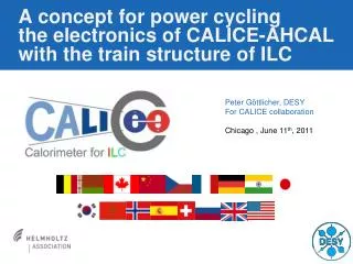
A concept for power cyclingthe electronics of CALICE-AHCAL with the train structure of ILC Peter Göttlicher, DESY For CALICE collaboration Chicago , June 11th, 2011
Outline • Introduction: ILC, ILD, AHCAL for CALICE • Motivation for power cycling • Building blocks for power cycling • Summary
Introduction Accelerator and Detector for e+e- ILC: International Linear Collider e+e- collider with 0.5 -1 TeV ILD: International Large Detector e+e- needs precise detectors Concept: Particle flow algorithm Measure showers of individual particles e+ Collision point with detectors e- • Technology: • Superdonductingcavitities 1.3 GHz • Bunch structure within trains • 1ms long trains, 199ms break, …. • bunch to bunch 337ns • Technology: • High granularity calorimeters • e.g. CALICE-AHCAL-barrel • 4 million readout channels • 60 thousand channels per m3 Option:For factor 100 by switching off the fast analogue electronics for 99.5% of the time Low power per channel: 40µW/channel can be reached by power cycling Need
Introduction AHCAL: Analog-Hadron- CALorimeter for ILD Sampling sandwich with 48 layers each 3 mm scintillator + 2.5 mm electronics, infrastructure +12 mm stainless steel Scintillator tiles with SiPM readout 3cm ASIC’s for - analogue signals, - local storage while train - ADC’s - data transfer Plugged to the back of a Readout board 12 x 12 tiles 36x36 cm2 Interconnects with flex foils for signals, GND and power Layer: composed out of 3 cassettes: 2600 channels Control electronics and power connections Cassette: 2.2m long structures: 864 channels
Motivation Motivation: Power Cycling to avoid active Cooling Mechanical design constraint: - No cooling within calorimeter to keep homogeneity and simplicity - Cooling only at service end • With • - Stainless steel • - Long structure • Heat • Electronics with • 1% power cycle • 25µW/channel • SiPMIdark • +15µW/channel • Need • Power cycling • To keep heat up below 0.50C Solution: Parabel + Fourier terms 0.3 Z=0m 0.2 0.1 Temperature increase [K] Z=2.2m • Simplified model: • No heat transfer radial • “bad due to sandwich” • Cylindrical symmetry • Symmetry at IP-plane 0.0 0.0 0.5 1.0 1.5 2.0 z = Position along beam axis [m]
Building blocks Building Blocks for the Power System DAQ is Optical: No issue for EMI 1. Planes with scintillators and SiPM’s, ASIC’s and PCB’s 4. Power supply 3. cable 2. End of layer electronics
Building blocks ASIC for fast SiPM Signals consuming Low Power L. Raux et al., SPIROC Measurement: Silicon Photomultiplier Integrated Readout Chips for ILC, Proc. 2008 IEEE Nuclear Science Symposium (NSS08) • Functional tasks of the ASIC: • Amplify the SiPM signal and generate self trigger • Store an identified signal: 16 per train: capacitor pipeline • Digitize • Multiplexed data transfer even with more ASIC’s Amp. Digital data transfer ADC 0.5% needed SiPM ASIC: SPIROC-2b RAM Algorithm for power cycling: The ASIC switches the current of the functional blocks OFF. ASIC gets supplied all the time with voltage. PCB electronics and instruments stabilize the voltage Bunches from collider (ILC/CLIC): A train every 200ms >20µs ON before train Fast amplifiers: 1ms Power ON for: ADC’s 3.2ms 1µs Common analogue parts, e.g. DAC’s, C-pipeline Digital control: 150ms
Building blocks ASICas current switch Measurements: - Inductive current probes Slow: 0.25 – 50MHz Fast: 30MHz-3GHz - Setup: ASIC+ capacitors on a PCB - Expectation is ~ 1mA/channel ~40mA/ASIC, summed over all pins Measured currents at the GND-supply of ASIC 10mA/pin GND pin (1 of 2) of ASIC Slow probe Tantal capacitor High pass of probe Expected waveform, Amplitude is arb. units. 0 200 400 600 [ns] time 30mA/pin GND pin (1 of 2) of ASIC Fast probe Voltage pin (1 of 3) for preamplifier • System has to deal with: • EMI: electromagnetic interference • 5Hz from train repetition to few 100MHz • 2.2A for a layer, 3.4kA for AHCAL-barrel -20 0 20 40 60 [ns] time
Building blocks Electro Magnetic Interference in a Power Cycled System • Reference ground: • Need good definition • Any induced/applied current produces voltage drops • Separation between reference / power return / safety • or controlling currents • and keeping currents within “own” volume and instrumentation return reference Safety. PE • Current loops • To do: • Controlling return currents • Keeping loops small • Avoid overlapping with • foreign components. • Capacitive coupling • To do: • Keep common mode voltage stable • Guide induces currents to source • Keep GND-reference closer • than foreigns Guideline: Avoiding emission avoids in most cases picking up of noise
Building blocks Keeping the high Frequencies local Simulation model: “two diomensional delay line” 36 x 36 cm PCB with scintillators, SiPM’s LED 144mA switched current Part of a thin cassette between absorber layer of HCAL 1cm x 1cm Layer structure of PCB: GND d PCB= 50-60µm Vsupply GND Capacitor well known: One-dimensional delay well known Inductivity: • By that one get • a thin PCB and also • A good high frequency capacitor 60pF/cm2 • Layout with short distance to via maintain the performance.
Building blocks Voltage for ASIC stabilized by local discrete Capacitors Capacitors mounted to the 36x36cm2 PCB Simulation of voltage induced by current ASIC is supported over wide frequency range with Z< 0.1W 144mA generates <20mV Oscillations are dumped for wide frequency range with phase ¹ ±900 Trust in simulation: - <1.5GHz=(1/10) granularity - No resistive behavior of ASIC is included. That over estimates the resonances at high frequencies Result: - Locally good for > 10kHz - Additional effort < 10kHz 100 W Ceramics X7R 10 W Murata, 100nf Murata, 1nf Murata, 10nf Tantal, AVX, 33µF Murata, 2.2nf PCB, alone 1 W Impedance Z=|U|/|I| 0.1 W Total: 12 Tantal/4 ASIC’s + 17 ceramics + PCB 00.1 W 900 Coil like U to I phase shift 00 Capacitor like -900 1GHz 1MHz 1kHz Frequency PCB-layer Tantal Dominated by: ceramic
Building blocks Low frequency charge storage for < 10kHz At end of layer, there is a bit of - space - cooling C2 C3 Concept: - Charge for the train stored in a capacitor C2 - Voltage drop allowed ~ 0.6V - Fast voltage regulator - Charge for faster reaction is within the distributed capacitors + C3 C2 = 3.4mF bank of few Tantal a voltage regulator with external FET > 2A C3+distributed = 2mF
Building blocks Voltage at ASIC: Measurement Reduced test setup: Control board, 1 interconnect, 1 board Definition of GND-point: - good for keeping sensitive SiPM’s stable - single connection to reduce currents in GNDPE system 2m2/Layer 1.3mm distance Stainless steel absorber = GNDPE C=13nF GNDelectronics Voltage step: - Measured 4mV, 400ns - Extrapolate to full system < 80mV at far end OK for operation, over-,undervoltage, time, … Induces current into GNDPE, if step is on GNDelectronics < 2 mA per layer 4mV Default setup Supplyvoltage of ASIC (AC-component) [mV] Tantal moved to control board Power on Command, step in IASIC Tantal taken away Control electronics for layer Time [ns] Þ OK, even with extrapolation to 1500 layers low? Investigations of reason and improvements possible, to be watched
Building blocks Integrating to Infrastructure 70pF/m from cable to support ASIC as switched current sink • Impact of cable • is a combination of choises: • Input filter: R=10W, C=1mF • reasonable mechanical size • EMI better t=100ms • Power supply behavior • here neglected capacitance • to PE, might be 2 order of • magnitude larger than cable! • Here: ideal V-source • Mechanical integration and galvanic isolation • per (group or) layer • and pair of wires for it 50m cable, 1mm2, on a cable support Current induced into GNDPE nA 0 -40 -80 -120 -160 Current per layer Simulation of cable 0 1 2 3 4 5 [ms] 6 time With 1500 layers of AHCAL: IPE=120mA Really small, but not including all parasitics! Don’t be too reluctant in EMI-rules
Building blocks Current in Supply Cable Reduced test setup: Control board, 1 interconnect, 1 board, Short cable to laboratory supply Preamplifiers ON ADC’s ON Work bench settings Without input filter with input filter t=10ms Current per 1/18 layer in supply cable [mA] Input filter important to lower amplitude fluctuations and remaining frequencies within cable Inportant: EMI-crosstalk to others Frequencies are low Electronics like to have larger t to smoothen further Û Mechanics easier in service-hall Control electronics for layer
Summary • Detectors for Linear Colliders requires many channels with low power • Train structure allows 99% time to be OFF: Factor 100 in critical regions • Coherent fast switching ON/OFF of high current: CALICE-AHCAL: 2.2A*layers : 3.4kA for the barrel 5Hz to few 100MHz • System aspects at local design - Local defined return-pathes for current - Local charge storage for wide frequency range that keeps - the impedance small - the currents leaving a defined volume small with slow rise times • System aspects within the infrastructure Lower frequency part handled by cables and power supply Good integration of power supplies and cables. • Simulation leaves many parasitic effects out Underestimates the high frequency EMI-disturbance …. Experiments, concepts to be better than simulation promises • Experimental setups and integration into ILD to be continued