Download
1 / 45
450 likes | 454 Vues
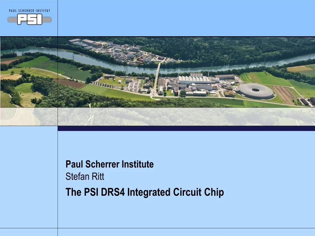
Stefan Ritt. Paul Scherrer Institute. The PSI DRS4 Integrated Circuit Chip. Agenda. Introduction to Switched Capacitor Array Chips Comparison with FADCs Overview of chips on the market The DRS4 chip Design principles Special features Some applications

E N D
Stefan Ritt Paul Scherrer Institute The PSI DRS4 Integrated Circuit Chip
Agenda Introduction to Switched Capacitor Array Chips Comparison with FADCs Overview of chips on the market The DRS4 chip Design principles Special features Some applications New ideas for DRS5 chip to be designed in 2011 Increased bandwidth Zero dead time DPP Workshop PSI
Introduction toSwitched Capacitor ArrayChips DPP Workshop PSI
Detectors in Particle Physics Particles interact with matter and produce light: Signal: ~ 100’s mV 10-100 ns DPP Workshop PSI
Flash ADC Technique Baseline Restoration Transimpedance Preamplifier PMT/APD Wire FADC “Fast”12 bit Digital Processing FADC Q-sensitive Preamplifier 60 MHz12 bit Shaper PMT/APD Wire Amplitude TDC Time • Shaper is used to optimize signals for “slow” 60 MHz FADC • Shaping stage can only remove information from the signal • Shaping is unnecessary if FADC is “fast” enough • All operations (CFD, optimal filtering, integration) can be done digitally DPP Workshop PSI
Nyquist-Shannon Theorem If a function x(t) contains no frequencies higher than F Hertz, it is completely determined by giving its ordinates at a series of points spaced 1/(2F) seconds apart. • If a detector produces frequencies up to 500 MHz (0.6 ns rise time), all information from that detector is recorded if sampled at 1 GSPS with good enough signal-to-noise ratio DPP Workshop PSI
How to measure best timing? Simulation of MCP with realistic noise and different discriminators K. Byrum, H. Frisch, J.-F. Genat et al., IEEE Trans.Nucl.Sci.57, 525 (2010) DPP Workshop PSI
Currently available fast ADCs 8 bits – 3 GS/s – 1.9 W 24 Gbits/s 10 bits – 3 GS/s – 3.6 W 30 Gbits/s 12 bits – 3.6 GS/s – 3.9 W 43.2 Gbits/s 14 bits – 0.4 GS/s – 2.5 W 5.6 Gbits/s 24x1.8 Gbits/s • Requires high-end FPGA • Complex board design • FPGA power 1.8 GHz! DPP Workshop PSI
ADC boards PX1500-4: 2 Channel3 GS/s8 bits ADC12D1X00RB: 1 Channel 1.8 GS/s 12 bits 1-10 k€ / channel DPP Workshop PSI
Switched Capacitor Array 0.2-2 ns Inverter “Domino” ring chain IN Waveform stored Out FADC 33 MHz Clock Shift Register “Time stretcher” GHz MHz DPP Workshop PSI
Switched Capacitor Array Cons No continuous acquisition Limited sampling depth Nonlinear timing Pros High speed (5 GHz) high resolution (11.5 bit) High channel density (9 channels on 5x5 mm2) Low power (10-40 mW / channel) Low cost (~ 10€ / channel) STRAW3 AFTER SAM DRS1 DRS2 TARGET DRS3 DRS4 LABRADOR3 MATACQ D. Breton E. Delagnes CEA Saclay G. Varner Univ. of Hawaii This talk Dt Dt Dt Dt Dt Goal: Minimize Limitations DPP Workshop PSI
The DRS4 Chip DPP Workshop PSI
CMOS process (typically 0.35 … 0.13 mm) sampling speed Number of channels, sampling depth, differential input PLL for frequency stabilization Input buffer or passive input Analog output or (Wilkinson) ADC Internal trigger Exact design of sampling cell Design Options PLL Trigger ADC DPP Workshop PSI
DRS History 1995 DSC Roger Schnyder, Christian Brönnimann, pb Tiny signal 20 pF 0.2 pF DRS1 2002 I Temperature Dependence ~kT 2004 DRS2 Roberto Dinapoli DRS3 2007 2008 DRS4 PLL-regulated Sampling Speed DPP Workshop PSI
DRS4 Fabricated in 0.25 mm 1P5M MMC process(UMC), 5 x 5 mm2, radiation hard 8+1 ch. each 1024 bins,4 ch. 2048, …, 1 ch. 8192 Passive differential inputs/outputs Sampling speed 700 MHz … 5 GHz On-chip PLL stabilization Readout speed 30 MHz, multiplexedor in parallel DPP Workshop PSI
12 bit resolution <8 bits effective resolution 11.5 bits effective resolution DPP Workshop PSI
Bandwidth Bandwidth is determined by bond wire and internalbus resistance/capacitance: 850 MHz (QFP), 950 MHz (QFN), ??? (flip-chip) ~2 nH Bond wire Parasitic ~10 pF finalbus width QFP package 850 MHz (-3dB) Simulation Measurement Ueli Hartmann DPP Workshop PSI
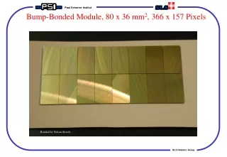
Bump Bonding Reduce input inductance by using bump bonding instead of wire bonding 200 mm 75 mm DPP Workshop PSI
How to minimize dead time ? Fast analog readout: 30 ns / sample Parallel readout Region-of-interestreadout Simultaneouswrite / read AD9222 12 bit 8 channels DPP Workshop PSI
ROI readout mode delayed trigger stop normal trigger stop after latency stop Trigger Delay 33 MHz e.g. 100 samples @ 33 MHz 3 us dead time 300,000 events / sec. readout shift register Patent pending! DPP Workshop PSI
Daisy-chaining of channels Domino Wave Domino Wave clock clock enable input enable input 1 Channel 0 0 Channel 0 enable input enable input 0 Channel 1 1 Channel 1 Channel 2 0 Channel 2 1 Channel 3 Channel 3 1 0 Channel 4 Channel 4 0 1 Channel 5 Channel 5 1 0 Channel 6 Channel 6 0 1 Channel 7 Channel 7 1 0 DRS4 can be partitioned in: 8x1024, 4x2048, 2x4096, 1x8192 cellsChip daisy-chaining possible to reach virtually unlimited sampling depth DPP Workshop PSI
readout Channel 0 1 Channel 0 1 0 1 Channel 1 Channel 1 Channel 2 Simultaneous Write/Read FPGA 0 Channel 0 0 Channel 1 8-foldanalog multi-eventbuffer Channel 2 0 Channel 3 0 Channel 4 0 Channel 5 0 Channel 6 0 Channel 7 0 Expected crosstalk ~few mV DPP Workshop PSI
DRS4 around the world Shipped (-Jan 2011): 2200 Chips 120 Evaluation Boards DPP Workshop PSI
MEG Experiment • MEG experiment @ PSI searches for meg decay • After ~10 years of chip design, DAQ setup, firmware programming, MEG runs with 3000 channels as designed • 40 ps timing resolutions between all channels, running at 1.6 GS/s • “Double buffer” readout mode increases life time to 99.7 % at 10 Hz event rate (3 MB/event) • Took 400 TB in 2010 DPP Workshop PSI
DRS4 @ MEG LMK03000 4 x DRS4 32 channels 3000 Channels DPP Workshop PSI
On-line waveform display S848 PMTs “virtual oscilloscope” template fit click pedestal histo DPP Workshop PSI
Crosstalk elimination Crosstalk removal by subtracting empty channel subtract Hit Hit DPP Workshop PSI
Template Fit Determine “standard” PMT pulse by averaging over many events “Template” Find hit in waveform Shift (“TDC”) and scale (“ADC”)template to hit Minimize c2 Compare fit with waveform Repeat if above threshold Store ADC & TDC values pb Experiment 500 MHz sampling DPP Workshop PSI
Trigger and DAQ on same board SCA can only sample a limited (1024-bin window) many application require a wider window, trigger capability would require continuous digitization Using a multiplexer in DRS4, input signals can simultaneously digitized at 120 MHz and sampled in the DRS FPGA can make local trigger(or global one) and stop DRSupon a trigger DRS readout (5 GSPS)though same 8-channel FADCs DRS4 MUX global trigger bus trigger FPGA DRS FADC12 bit 65 MHz analog front end LVDS SRAM DPP Workshop PSI
“Slow” waveform and “Fast” window TriggeredDRS Waveform 1 GSPS (1 ns bins) up to 5 GSPS Window only limited by RAM Continuous Waveform 120 MSPS (8 ns bins) DPP Workshop PSI
Sine Curve Fit Method i yji : i-th sample of measurement j aj fj ajoj : sine wave parameters bi : phase error fixed jitter • “Iterative global fit”: • Determine rough sine wave parameters for each measurement by fit • Determine bi using all measurements where sample “i” is near zero crossing • Make several iterations j S. Lehner, B. Keil, PSI DPP Workshop PSI
Fixed Pattern Jitter Results • TDi typically ~50 ps RMS @ 5 GHz • TIi goes up to ~600 ps • Jitter is mostly constant over time, measured and corrected • Residual random jitter 3-4 ps RMS • Achievable resolution exceeds best CFD + HPTDC DPP Workshop PSI
Time-of-Flight PET • Conventional electronics:CFD – TDC: 500 ps RMS • TOF needs: • 100-200 ps • >1 MHz rate C. Levin, Stanford University DPP Workshop PSI
ToF-PET Project • Started fall 2010 after NSS/MIC in Knoxville (Siemens PET R&D home) • New project started to replace current PET electronics with DRS4 (5) • PCB ready summer 2011, firmware by Univ. Tübingen • Simulations show that SCA technique can achieve 100 ps easily FPGA “Ping-Pong Scheme” 1 Channel 0 Channel 0 ROI 0 Channel 1 Channel 1 Channel 2 0 20 samples (10 ns @ 2 GS/s) * 30 ns / sample = 600 ns + 40 ns overhead = 640 ns 1 MHz rate Channel 3 0 Channel 4 0 Channel 5 0 Channel 6 0 Channel 7 0 DPP Workshop PSI
DRS5 Chip Ideas DPP Workshop PSI
Plans for DRS5 Increase analog bandwidth ~5 GHz Smaller input capacitance Increase sampling speed ~10 GS/s Switch to 110 nm technology Deeper sampling depth 8 x 4096 / chip Minimize readout time (“dead time free”) for muSR & ToF-PET (minor) reduction in analogreadout speed (30 ns 20 ns) Implement FIFO technology J. Milnes, J. Howoth, Photek mSR ~MHz event rate CTA DPP Workshop PSI
Next Generation SCA Low parasitic input capacitance High bandwidth Large area low resistance bus, lowresistance analog switches high bandwidth Short sampling depth Deep sampling depth • Digitize long waveforms • Accommodate long trigger delay • Faster sampling speed for a given trigger latency How to combine best of both worlds? DPP Workshop PSI
Cascaded Switched Capacitor Arrays input shift register • 32 fast sampling cells (10 GSPS/110nm CMOS) • 100 ps sample time, 3.1 ns hold time • Hold time long enough to transfer voltage to secondary sampling stage with moderately fast buffer (300 MHz) • Shift register gets clocked by inverter chain from fast sampling stage . . . . . . . . . . . . . . . . . . . . . . . . . . . . . . . . . fast sampling stage secondary sampling stage DPP Workshop PSI
How noise affects timing voltage noise band of signal voltage noise Du signal height U timing jitter arising from voltage noise timing uncertainty Dt rise time tr timing jitter is much smaller for faster rise-time number of samples on slope DPP Workshop PSI
TDC vs. Waveform Digitizing Constant Fraction Discriminator Q-sensitive Preamplifier Shaper PMT/APD Wire TDC • CFD and TDC on same board crosstalk • CFD depends on noise on single point,while waveform digitizing can average over several points • Inverter chain is same both in TDCs and SCAs • Can we replace TDCs by SCAs? yes if the readout rate is sufficient DPP Workshop PSI
Typical Waveform Only short segments of waveform need high speed readout DPP Workshop PSI
Dead-time free acquisition Self-trigger writing of short 32-bin segments Simultaneous reading ofsegments Quasi dead time-free Data driven readout Ext. ADC runs continuously ASIC tells FPGA when there is new data Coarse timing from300 MHz counter Fine timing by waveformdigitizing and analysis in FPGA 20 * 20 ns = 0.4 ms readout time 2 MHz sustained event rate Attractive replacement for CFD+TDC DRS5 DPP Workshop PSI
Plug & Play Firmware Emphasis shift from dedicated hardware to firmware Pre-designed modules for CFD, TDC, peak sensing ADC, … Modules can be configured by user and downloaded TDC FIFO CFD ADC Readout SCALER Interface FIFO FIFO ADC FIFO Data bus Parameter bus DPP Workshop PSI
Conclusions DRS4 chip successfully used in many areas, true potential of SCA technology is just now discovered Planned DRS5 chip will increase BW and decrease readout dead time SCA technology should be able to replace most traditional electronics in particle detection DPP Workshop PSI
Thanks to … Roland Horisberger: Original Idea Roberto Dinapoli: Analog Design of DRS3+4 Ueli Hartmann: DRS4 Evaluation Boards PSI chip design core team DPP Workshop PSI