Download
1 / 52
570 likes | 847 Vues
Clock Distribution. based on Dennis Sylvester at Univ. Michigan www.eecs.umich.edu. Contents. Introduction Clock Power Clock Distribution for Uniform Delay Clock Integrity. Function of clock distribution network. Synchronize millions (billions) of separate elements

E N D
Clock Distribution based on Dennis Sylvester at Univ. Michigan www.eecs.umich.edu
Contents • Introduction • Clock Power • Clock Distribution for Uniform Delay • Clock Integrity
Function of clock distribution network • Synchronize millions (billions) of separate elements • Within a time scale on order of ~10 ps • At distances spanning 2-4 cm • Ratio of synchronizing distance to element size on order of 105 • Reference: light travels <1 cm in 10 ps
Metrics/Goals • Besides basic connectivity, what makes a clock network good or bad? • Skew • Jitter • Power • Area • Slew rates
Clock Skew • The most “high-profile” of the clock network metrics • Defined as: Maximum difference in arrival times of clock signal to any 2 latches/FF’s fed by the network Skew = max | t1– t2 |
Clock Skew • Causes: • Designed (unavoidable) variations – mismatch in buffer load sizes, interconnect lengths • Process variation – process spread across die yielding different Leff, Tox, etc. values • Temperature gradients – changes MOSFET performance across die • IR voltage drop in power supply – changes MOSFET performance across die • Note: Delay from clock generator to fan-out points (clock latency) is not important by itself • BUT: increased latency leads to larger skew for the same amount of relative variation
Cycle time Clock Skew • Effect: • Eats into timing budget • Needs to be considered for maximum (setup) and minimum (hold) path timings Ref : Simplex website
NOTES : JITTER J1 = t2 – t1 JITTER J2 = t3 – t2 Jitter • Clock network delay uncertainty • From one clock cycle to the next, the period is not exactly the same each time • Maximum difference in phase of clock between any two periods is jitter
Jitter • Caused by variations in clock period that result from: • Phased-lock loop (PLL) oscillation frequency • Various noise sources affecting clock generation and distribution • Ex. Power supply noise which dynamically alters the drive strength of intermediate buffer stages • Jitter can be reduced by minimizing power supply noise (IR and L*di/dt)
Jitter Impact on Timing Budget • Needs to be considered in maximum path timing (setup) • Typically on the order of 50ps in high-end microprocessors
Clock Power • Power consumption in clocks due to: • Clock drivers • Long interconnections • Large clock loads – all clocked elements (latches, FF’s) are driven • Different components dominate • Depending on type of clock network used • Ex. Grid – huge pre-drivers & wire cap. drown out load cap.
Clocks: Power-Hungry Not only is the clock capacitance large, it switches every cycle! P = α C Vdd2 f
Low Power Clocking Techniques • Gated clocks • Prevent switching in areas of the chip not being used • Easier in static designs • Edge-triggered flip-flops in ARM rather than transparent latches in Alpha • Reduced load on clock for each flip-flop as well as eliminated spurious power-consuming transitions during flow-through of latches
Clock Distribution Metric: Area • Clock networks consume silicon area (clock drivers, PLL, etc.) and routing area • Routing area is most vital • Top-level metals are used to reduce RC delays • These levels are precious resources (unscaled) • Power routing, clock routing, key global signals • By minimizing area used, we also reduce wiring capacitance & power • Typical #’s: Intel Itanium – 4% of M4/5 used in clock routing
Slew Rates • To maintain signal integrity and latch performance, minimum slew rates are required • Too slow – clock is more susceptible to noise, latches are slowed down, eats into timing budget • Too fast – burning too much power, overdesigned network, enhanced ground bounce • Rule-of-thumb: Trise and Tfall of clock are each between 10-20% of clock period (10% - aggressive target) • 1 GHz clock; Trise = Tfall = 100-200ps
Slew Rates • Latch set-up times are dependent on clock input slew rates (eats into timing budget) • Short-circuit power grows with larger slew rates • This can be significant for large clock drivers Ref : IBM sebsite, Carring
Clock Distribution Example Alpha 21264 clock distribution -- grid + H- tree approach Power = 32% of total Wire usage = 3% of metals 3 & 4 4 major clock quadrants, each with a large driver connected to local grid structures
Technology Trends: Timing • Clock period dropping fast, so skew must follow accordingly • Slew rates must scale with cycle time also • Jitter – PLL’s get better with CMOS scaling • but other sources of noise increase • Power supply noise more important • Switching-dependent temperature gradients
Technology Trends: NewInterconnect Materials Copper reduces RC slew degradation and potential skew Low-k dielectrics decrease clock power and improve latency/skew/slew rates Ref: IBM, JSSCC, 11/
Technology Trends: Power • Heavily pipelined design more latches, more capacitive load for clock • Larger chips more wire-length needed to cover the entire die • Complexity more functionality and devices means more clocked elements • Dynamic logic more clocked elements
Fundamental Design DecisionPower vs. Skew • Meeting skew requirements is relatively easy… With an unlimited power budget! • Ex. Wide wires – minimize RC product but increase total C • Ex. Size up drivers – limit latency (translates to skew) but buffer cap. jumps
SoC power requrements • SoC’s have more stringent power limitations due to packaging constratints • Plastic packaging, power ~ 2-3 W • This pushes the skew-power tradeoff towards higher skew • Intolerable considering the drive for high performance • SoC’s are good candidates for power-friendly skew-reducing “tricks”
Network Types: Grid • Gridded clock distribution was common on earlier DEC Alpha microprocessors • Advantages: • Skew determined by grid density and not overly sensitive to load position • Clock signals are available everywhere • Tolerant to process variations • Usually yields extremely low skew values Pre-drivers Global grid
Grid Disadvantages • Huge amounts of wiring & power • Wire cap large • Strong drivers needed – pre-driver cap large • Routing area large • To minimize all these penalties, make grid pitch coarser • Skew gets worse • Losing the main advantage • Don’t overdesign – let the skew be as large as tolerable • Still – grids seem non-feasible for SoC’s
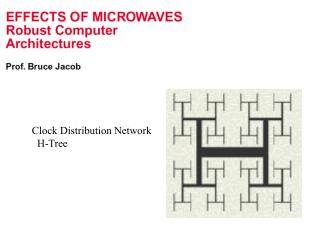
Network Types: Tree • Original H-tree (Bakoglu) • One large central driver • Recursive H-style structure to match wire-lengths • Halve wire width at branching points to reduce reflections
H-Tree Problems • Drawback to original tree concept • slew degradation along long RC paths • unrealistically large central driver • Clock drivers can create large temperature gradients (ex. Alpha 21064 ~30° C) • non-uniform load distribution • Inherently non-scalable (wire resistance skyrockets) • Solution to some problems • Introduce intermediate buffers along the way • Specifically at branching points
Buffered H-tree • Advantages • Ideally zero-skew • Can be low power (depending on skew requirements) • Low area (silicon and wiring) • CAD tool friendly (regular) • Disadvantages • Sensitive to process variations • Local clocking loads are inherently non-uniform
Balancing a Tree • Some techniques: • (a) Introduce dummy loads • (b) Snaking of wirelength to match delays Con: Routing area often more valuable than Silicon
Clock Skew and Clock balancing • Clock skew • Hold time violation is critical to working silicon • Aggressive skew budget for high speed operation • Large turn-around-time for clock tree synthesis at P&R stage • Skew Source : process + voltage + temp + load + jitter} • Skew Budget == ( Target Cycle Time ) /20 , min clk->Q • Solution • CTS (Clock Tree Synthesis) • Insert dummy delay at Synthesis Over-design
Clock tree style 3 Fanout Balance Tree Model 1 H-Tree Model Less flexible Net applicable to placement Easy to construct Weak for blest latch distribution 4 Spine and trunk Model (Fish and Bone) 2 Binary Tree Model Skew Hardly influenced by Process Scattering Die size increase Easy to adjust Net Loading Many dummy cells are needed
Practical problem in Clock tree synthesis • Problems • Large chip size due to SOC integration • # of FF’s = enormous, memory • Unbalanced FF distribution • Top-level : Interconnect RC dominant • Block-level : turn-around-time • Iteration cost • Test clock • Multiple clock frequency • Solution • Plan from the early design stage • Skew budgeting : 100ps @ 200MHz
Block level clock tree • Block-level clock skew • Driver-limited • Optimization of the buffer strength and number • Clock tree synthesis • Commercial tool -- P&R stage • Many iterations • Long turn-around-time • Clock tree planning • Virtual clock tree generation • Need engineering approximation
Real Clock Tree clk.4.1 clk.5.1 clk.3.1 Clock tree style Trunk-and-Branch
Virtual Clock Tree Model • Assumption :Uniform distribution of clock buffers and flip-flops • Model : Hierarchical trunk-and-branch L4 CLK buffer L3 CLK buffer * * * from L2 buffer N=6 N=7 N=8
Top Level Clock Distribution PLL NW NE L2 SS SE SW system
Clock Integrity • Shield everywhere • Laterally and above/below • Provide current return paths and eliminate coupled noise effects (both C and L ) Vdd GND CLK Vdd GND
Clock Integrity • di/dt for clock drivers can be enormous • All clocks should be switching at the same instant • Potential for L*di/dt noise on power supply • Explicit decoupling capacitance has been taken as solution to this problem • Thin gate oxides used in silicon white space to create large (100+nF) capacitance to supply charge • Alpha 21264 required additional decoupling capacitance at package level to limit switching noise (!)
Clock Shielding • How much does shielding help? Or reference planes? • Is it worth the area penalty?
Impact of Reference Planes in Power Distribution Conditions not given! Aluminum
Clock Grid Simulations /Reference Planes Copper wiring allows for smaller wires, finer grid pitch, lower power Eliminating need for reference planes
Reduce Self Inductance Dedicated Ground Planes G c Dedicated G.P. W G Wg
Guard Traces vs. Reference Plane • Below 5GHz, guard traces appear better
LF Current Distribution Current Spreads Through outer Bigger Current Loops
HF Current Distribution • Current Concentrates Underneath Signal Line Smaller Current Loops, and Smaller Inductance
Network of choice in high performance • Globally – Tree • Why? • Power requirements are reduced compared to global grid • Smaller routing requirements, frees up global tracks • Trees are easily balanced at the global level • Keeps global skew low (with minimal process variation)