Download
1 / 1
10 likes | 130 Vues
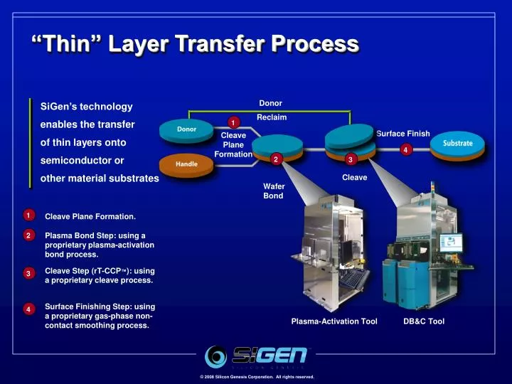
1. 2. 3. 3. 2. 4. 4. 1. “Thin” Layer Transfer Process. Donor Reclaim. SiGen’s technology enables the transfer of thin layers onto semiconductor or other material substrates. Surface Finish. Cleave Plane Formation. Wafer Bond. Cleave. Cleave Plane Formation.

E N D
1 2 3 3 2 4 4 1 “Thin” Layer Transfer Process Donor Reclaim SiGen’s technology enables the transfer of thin layers onto semiconductor or other material substrates Surface Finish Cleave Plane Formation Wafer Bond Cleave Cleave Plane Formation. Plasma Bond Step: using a proprietary plasma-activation bond process. Cleave Step (rT-CCP™): using a proprietary cleave process. Surface Finishing Step: using a proprietary gas-phase non-contact smoothing process. . Plasma-Activation Tool DB&C Tool